



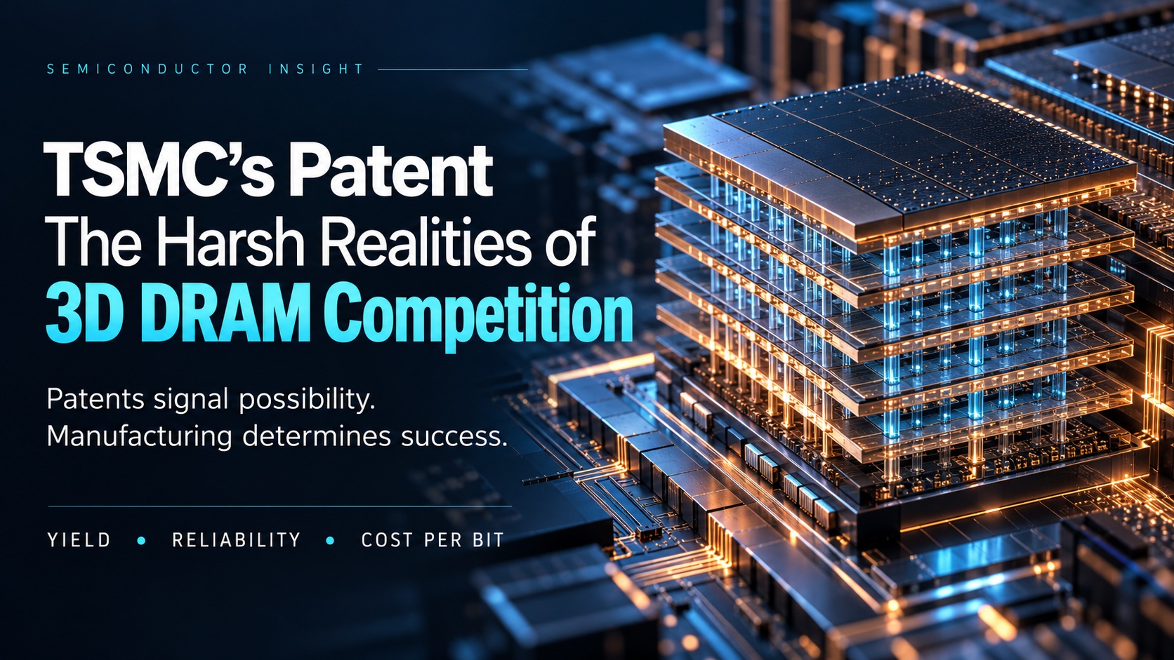
Discussions around TSMC’s vertical DRAM patents raise an intriguing question: could the world’s leading foundry eventually challenge established memory manufacturers? The curiosity is understandable. Patent disclosures involving vertical transistors and integrated capacitors show that TSMC is exploring architectures relevant to future memory scaling. But technical exploration and commercial market entry are different milestones, separated by enormous manufacturing and economic hurdles.
Precision matters when interpreting the patent itself. “US @2022” does not uniquely identify a document. One relevant TSMC application, US20220359529A1, published in November 2022, describes a vertical-channel transistor integrated with a hybrid trench-and-stacked capacitor. Another, filed in May 2022 and published as US20230240066A1, places a capacitor directly above a vertical gate-all-around transistor. These disclosures should not be merged into a single architecture or treated as product announcements.
Their significance is nevertheless real. They demonstrate exploration of ways to reduce memory-cell footprint and integrate storage structures vertically. They do not establish TSMC’s production readiness, investment commitment, or intention to sell commodity DRAM. A plausible interpretation is that such research preserves options for embedded memory, logic-memory integration, or future customer requirements. That remains an inference, rather than a disclosed commercial strategy.
The broader competitive story concerns how DRAM can continue scaling. SK hynix has publicly identified both a 4F² vertical-gate platform and 3D DRAM as future directions. Crucially, these are related but distinct concepts: a smaller cell footprint does not automatically mean multiple active memory layers. Likewise, stacking completed DRAM dies in HBM differs from building vertically repeated cells within a memory array.
For SK hynix, Samsung, Micron, and any prospective entrant, the decisive challenge is converting structural promise into reliable, affordable bits. A compelling cross-section is only the beginning. Engineers must make the transistor, capacitor, interconnects, and surrounding circuitry work together across large arrays, manufacturing variations, operating temperatures, and repeated production cycles.
The first obstacle is electrical control. An access transistor must deliver enough current for fast operation while limiting leakage sufficiently to preserve stored charge. Dense vertical arrangements also make interactions between neighboring structures harder to manage. SK hynix’s research on bit-line shielding and back-gate control illustrates how much engineering can sit behind an apparently simple reduction in cell area.
The second obstacle is capacitor integration. Shrinking the footprint does not remove the need for a readable charge-storage signal. Designers must balance capacitance, dielectric leakage, breakdown reliability, and fabrication complexity. Vertical geometry offers additional surface area, but it also demands consistent deposition, etching, and electrical connections in increasingly confined spaces. Every additional structural advantage introduces another integration problem that must be solved.
The third obstacle is manufacturing economics. Additional layers can increase nominal density while adding process steps, inspection requirements, and opportunities for defects. Thermal budgets constrain which materials and fabrication sequences can coexist. Bonding approaches introduce their own alignment and interface requirements. The relevant commercial measure is therefore cost per usable, qualified bit, rather than the number of cells drawn into a proposed structure.
This is why the patent discussion matters beyond speculation about TSMC. If conventional DRAM scaling becomes more difficult, architectural transitions could influence memory capacity, power consumption, supply economics, and the cost of computing. Yet higher density alone cannot guarantee greater bandwidth or lower system energy. Those outcomes also depend on peripheral circuits, interfaces, packaging, and how memory connects to processors.
Bottom line: TSMC’s disclosures deserve attention as evidence of technical exploration. Their larger lesson is that future DRAM leadership will require architecture, materials, process integration, and manufacturing discipline to advance together. Established memory companies bring accumulated production experience; potential challengers may bring different integration strengths. The winners will be those that turn promising structures into dependable products at competitive cost. That is where 3D DRAM competition becomes consequential.
Also Read:
TSMC’s AI Expansion Signals a Broader Shift in Computing
TSMC 2026 OIP Ecosystem Forum Summary
From Cloud to Silicon: IC-Link and TSMC Open the Door
Share this post via:


Comments
One Reply to “TSMC’s Patent and the Harsh Realities of 3D DRAM Competition”
You must register or log in to view/post comments.