





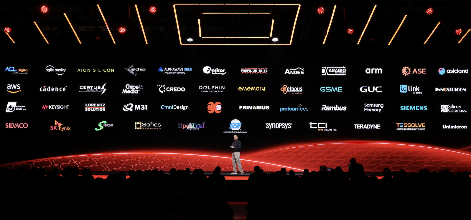
The 2026 TSMC Open Innovation Platform (OIP) Ecosystem Forum was held on September 23, 2026, in Santa Clara, CA. This is the event where TSMC showcases the substantial progress made with its massive semiconductor ecosystem. As one would expect, AI was a key topic throughout the day, with some very impressive results reported and some exciting exhibits from both established and new companies.
You can get an excellent overview of the entire event on SemiWiki here. In this post, I will cover the opening remarks delivered by two of TSMC’s executives. These presentations set the stage for what followed. It was a packed day of memorable presentations and eye-catching exhibits. So, let’s examine the TSMC OIP Ecosystem Forum 2026 opening remarks
Sajiv Dalal Kicks Off the Day
Sajiv Dalal is the President and Chief Executive Officer of TSMC North America. In the graphic at the top of this post, you can see him on the massive stage, surrounded by so many partner logos.
Artificial intelligence is no longer a future trend. It is already transforming industries, driving massive infrastructure investment, and creating an entirely new wave of semiconductor innovation.
That was the message from Sajiv at the opening of TSMC’s 2026 OIP Ecosystem Forum, where he pointed to an industry that has now crossed the $1.7 trillion mark and to AI infrastructure spending that he said reached roughly $1 trillion this year. Over the next several years, that investment is expected to grow dramatically as AI becomes increasingly embedded in both business and everyday life.
He explained that the impact extends far beyond data centers. AI is moving rapidly toward the edge, accelerating advances in drug discovery, diagnostics, autonomous vehicles, manufacturing, warehousing, and countless other applications. Behind that progress is an increasingly sophisticated semiconductor technology stack spanning advanced process nodes, chiplets, packaging, interconnects, memory, power delivery, and system integration.
TSMC is positioning itself at the center of that transformation. Dalal highlighted innovations including nanosheet technologies, advanced stacking and packaging, next-generation HBM base die, backside power delivery, and integrated voltage regulation—all aimed at delivering the performance and power efficiency required by increasingly demanding AI systems.
But perhaps the most important theme of his speech was collaboration.
Dalal stressed that semiconductor innovation at this scale cannot happen in isolation. TSMC’s Open Innovation Platform brings together a broad ecosystem of partners that collaborate early, co-optimize technologies, and work toward first-time silicon success.
The forum itself reflects that philosophy, bringing together TSMC technologists, customers, and partners for market outlooks, technical deep dives, and dozens of presentations across AI/HPC, mobile, automotive, and other applications.
The takeaway was clear: AI may be driving the semiconductor industry’s next major growth cycle, but collaboration across the ecosystem will determine how quickly—and successfully—that opportunity becomes reality.
Dr. Lipen Yuan Expands on the Vision
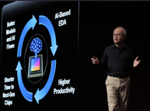
Dr. Lipen Yuan is Vice President, Business Development at TSMC. He began by pointing out that:
AI is not simply creating a new class of semiconductor products—it is forcing the industry to rethink how chips are designed, integrated, and brought to market. Dr. Yuan framed this shift as both an extraordinary growth opportunity and a fundamental engineering challenge: the next phase of AI will require innovation across the entire technology stack, backed by a much more tightly integrated ecosystem.
The scale of the opportunity is already visible. Dr. Yuan described what he called a “golden era” for semiconductors, noting that an industry once expected to reach the $1 trillion milestone around 2030 has moved dramatically faster as AI demand has surged, with the market now approaching $1.7 trillion.
At the center of TSMC’s strategy is its Open Innovation Platform (OIP), which has spent nearly two decades bringing together foundry technology, EDA tools, intellectual property, cloud infrastructure, design services, packaging, and manufacturing expertise. Dr. Yuan pointed out that this collaborative model has helped lower barriers to chip development and enabled innovators worldwide to turn advanced semiconductor technologies into differentiated products.
That ecosystem is becoming even more important as AI moves beyond the cloud into edge devices, automotive systems, physical AI, and other emerging applications. These workloads are driving enormous increases in compute demand while simultaneously placing pressure on memory bandwidth, interconnect performance, power consumption, cooling, and system efficiency.
According to Yuan, the industry can no longer optimize individual chips in isolation. Future AI platforms will require system-wide co-design spanning advanced logic, packaging, memory, interconnects, power delivery, cooling, and networking. TSMC therefore sees the industry expanding from traditional design-technology co-optimization, or DTCO, toward broader system-technology co-optimization, or STCO.
Advanced packaging is another critical part of this shift. Yuan highlighted TSMC’s 3DFabric Alliance, which brings together memory, EDA, test, OSAT, and other partners to address the thermal, mechanical, and integration challenges associated with increasingly complex multi-die systems.
But perhaps the most forward-looking portion of the speech focused on using AI itself to design the chips that power AI.
Yuan said TSMC is already seeing meaningful productivity gains from AI-assisted semiconductor design. The company is now taking the next step with the introduction of the TSMC AI Design Kit, or ADK. Designed to complement traditional process design kits and established EDA flows, the ADK is intended to support emerging agentic AI design methodologies. TSMC envisions a future in which engineering teams create orchestration layers of AI agents and specialized skills that work alongside—or potentially replace portions of—traditional CAD flows.
The broader message was clear: scaling AI is no longer simply a matter of building faster silicon. It is becoming a system-level engineering challenge that requires deeper collaboration across the entire semiconductor ecosystem.
For TSMC and its partners, the opportunity is not simply to build chips for the AI revolution, but to use AI, advanced packaging, and system-level optimization to reinvent how those chips are designed in the first place.
To Learn More
There will be more posts on TSMC OIP Ecosystem Forum 2026. The event delivered rich content across many aspects of advanced chip development and highlighted the achievements of TSMC’s ecosystem partners. You can access an overview of TSMC OIP here. And that’s a summary of the TSMC OIP Ecosystem Forum 2026 opening remarks.
Also Read:
Designing chips for the AI era: what TSMC’s roadmap means
The Intelligence Revolution: TSMC’s OIP Ecosystem Forges the Path to Trillion-Transistor AI Systems
Podcast EP368: An Overview of TSMC Open Innovation Platform (OIP) event with Aveek Sarkar
Comparison of TSMC CoWoS-S, CoWoS-R, and CoWoS-L
Share this post via:



Comments
There are no comments yet.
You must register or log in to view/post comments.