





The semiconductor industry crossed $1 trillion in annual revenue this year, almost four years ahead of earlier projections. SEMI President and CEO Ajit Manocha opened the CEO Summit at SEMICON West with a chart that told the story. A year ago, the forecast for 2030 was $1 trillion. Now it is $2 trillion, with $3 trillion possible by 2035. The industry has 102 new fabs coming online through 2029 and needs more than 50 beyond that by 2035.
Money and capacity won’t carry that growth alone. Synopsys CEO Sassine Ghazi named the shortage of engineers as the industry’s challenge. Brooks Automation CEO Dave Jarzynka pointed out that a wafer spends only about 25% of its time in the fab actually being processed. AMD’s Justin Murrill summed up the mood in two lines: “Constraints don’t prevent progress. They guide where the next breakthrough comes from.”
The question underneath it all was how to deliver more, faster, with the people and factories we have. I spent Tuesday, October 13, in Room 20 at Moscone North for the design session, “Bridging Design and Manufacturing with AI,” and it took that question on directly. Speakers from TSMC, Intel, Applied Materials, Lam Research, Cadence, Silvaco, PDF Solutions, McKinsey, Cerebras, SanDisk, and VerifAIX covered everything from atoms to agents. Seven themes stood out:
- AI is expanding the solution space
- AI’s real payoff is faster learning, not cost reduction
- AI is compressing the steps, and the time between them is the next frontier
- Co-optimization is replacing the sequential handoff
- Design is speeding up, manufacturing is not
- Autonomous design is causing trust issues
- Digital twins are changing how development gets done
AI is expanding the solution space. Lam Research’s David Fried put the number of possible process recipes on the order of 10²³. Intel’s Vikas Sharma showed a design-technology co-optimization (DTCO) search space that grew from fewer than 10 options to more than a million. Applied Materials’ Subi Kengeri described thousands of materials candidates and hundreds of coupled variables per study. No team of engineers can explore that many options on their own. ML finds the parameters that matter, and AI finds the best candidates to try.
AI’s real payoff is faster learning, not cost reduction. Sandisk said it plainly on the IEEE panel moderated by Silvaco’s Wally Rhines: AI narrows ten candidates to three before design starts, with fewer experiments and shorter cycles, and the value is speed. Intel’s DTCO decisions dropped from weeks to one or two hours. Applied Materials cut a 3D gate-all-around device simulation from 20.5 days to 19.7 hours on GPUs. Every one of these is a learning loop getting shorter.
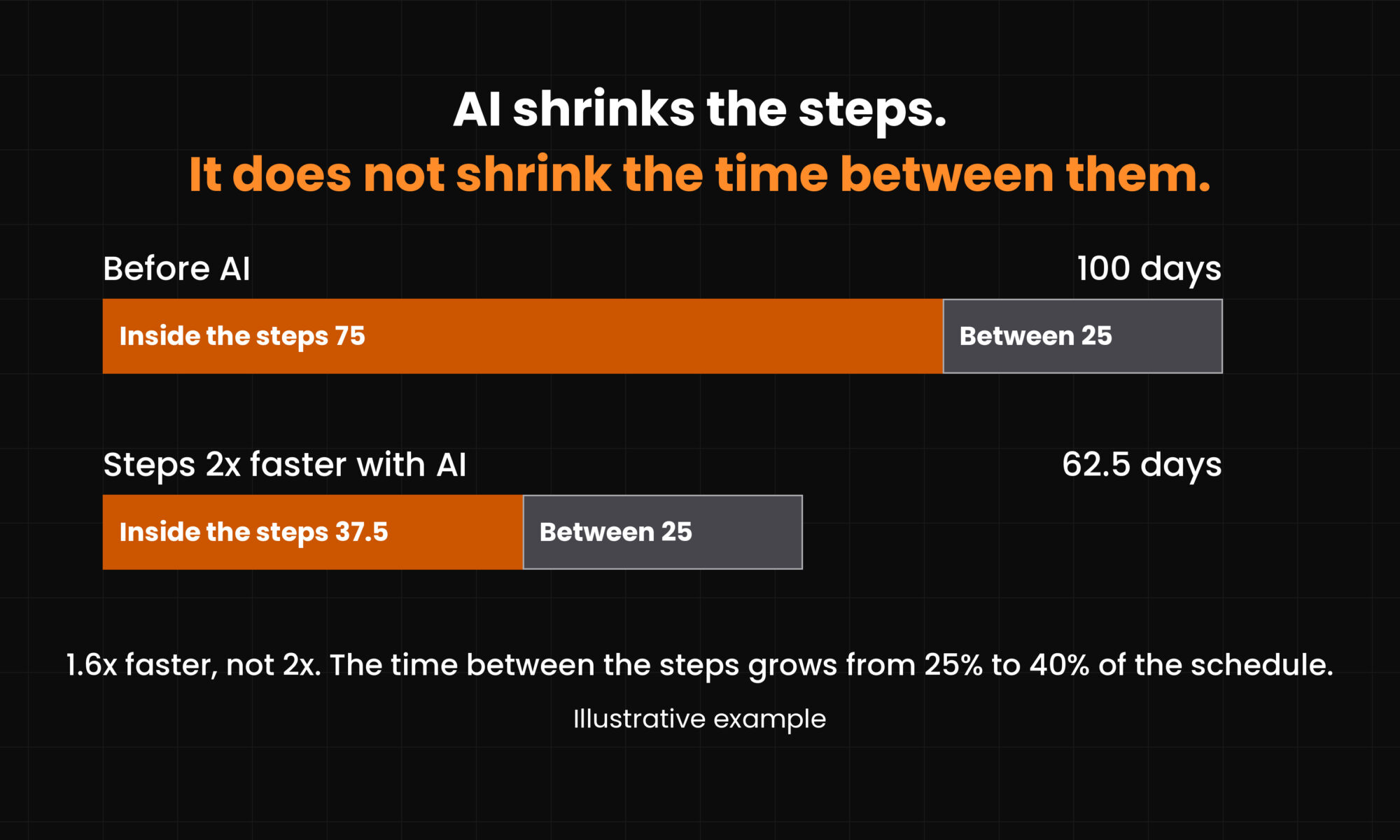
AI is compressing the steps, and the next frontier is the time between them. Cycle time inside the steps is falling fast. McKinsey showed AI-assisted programs reaching tape-out nine months after design starts and cutting debug closure time by 40%. TSMC’s agentic place-and-route runs around the clock at 3 to 5x productivity. McKinsey’s Aaron Aboagye added a related point: a meaningful share of development latency is organizational, not physical, and orchestration compresses the white space between technical steps. PDF Solutions showed test data that rarely follows the product downstream. Brooks’s 25% is the same pattern in the fab: most of a wafer’s time is spent between the steps, not in them.
I’d take McKinsey’s point one step further. As AI compresses the time inside the steps, the time between them, team to team and team to tool, becomes a bigger share of the schedule. From inside a program, that time has a cause: how the work between the steps is designed. In most programs, it was never designed at all.
Co-optimization is replacing the sequential handoff DTCO, and system-technology co-optimization (STCO) says the same thing: design, process, package, and system decisions get made together, not passed down a line. Applied Materials described STCO as one coupled loop, with constraints flowing down and outcomes flowing up. Intel showed that degrees of freedom and reversibility shrink as the PDK matures, so the right decisions must come early. Cerebras showed co-optimization at wafer scale, engineering the wafer, DRAM, and optics together and coupling every design domain. TSMC is moving from the PDK to an AI Design Kit built for agents. McKinsey called for persistent, cross-stack co-development in place of sequential handoffs.
System complexity keeps rising, and engineers have had to rise with it. Technical depth used to be enough. Then we needed breadth. Now we need to understand the whole system. Co-optimization is the latest answer to that pressure, and as complexity grows, it will have to keep evolving.
Design is speeding up; manufacturing is not. Manufacturing can’t iterate without physical consequences, and the physics keeps getting harder. Transistors have gone from planar to FinFET to gate-all-around, with CFET and 2D materials next. Rhines showed NAND process steps rising from about 400 to as many as 1,800, wafer lot cycle time stretching from 8 to 10 weeks at 28nm to 16 weeks or more, and mask sets climbing from $1 to 3 million to $20 to 40 million or more. McKinsey’s view: manufacturing remains largely uncompressed.
Autonomous design is causing trust issues. VerifAIX’s Madhulima Tewari called it the correctness gap. She cited first-silicon success at 14% and the best AI pass rate on hardware code generation at 34% and argued that the system that generates an artifact can’t be the only one that certifies it. Her answer: the LLM proposes, deterministic engines decide. Cadence’s Jeff Roane said agentic AI is here now, with one to two years to figure out how to use it well. At the CEO Summit, Ghazi described the end state: you give an outcome, not a prompt, and human judgment still defines the architecture.
Digital twins are changing how development gets done. Systems are getting harder for any one engineer to understand, which is why digital twins are becoming so important. Models and virtual prototypes help development teams see how the pieces interact. Physical prototypes teach the same lessons, but every learning cycle on silicon costs weeks and millions of dollars. Rhines called the virtualization of manufacturing inevitable. Physics simulation trains surrogate models that let teams test process changes before running a wafer. Lam builds virtual twins of process and fab, and Applied Materials uses the same surrogate pattern from materials to system. The twins run on data, and the data is exploding. PDF Solutions’ Kimon Michaels cited Qualcomm’s engineering and manufacturing data growing 600% since 2022, while less than 5% of manufacturing data gets analyzed. A twin is only as good as its calibration.
Across all seven themes, the pattern was the same: AI is making each step faster and each search smarter. Lam’s own research, published in Nature, put the lesson plainly: engineers and algorithms working together, with the handoff in the right place, cut the cost of reaching a process target in half. That handoff is a design decision, and so is every other boundary in the flow, between design and manufacturing, between teams, between companies. When an agent can run place-and-route around the clock, your schedule stops being set by how fast your engineer works. It is set by how fast decisions, data, and learning move across those boundaries. The $1 trillion was built on faster tools. The next trillion goes to the companies that design how their people and tools work together.
Also Read:
Accellera’s FSL 1.0 Gives Functional Safety Data a Common Language
SEMICON West 2026: After the Toast, the Hard Questions
WEBINAR: Cut down EDA License cost by 25% with Stratos AI Nitro
Share this post via:


Why America’s Semiconductor Manufacturing Capacity Matters