




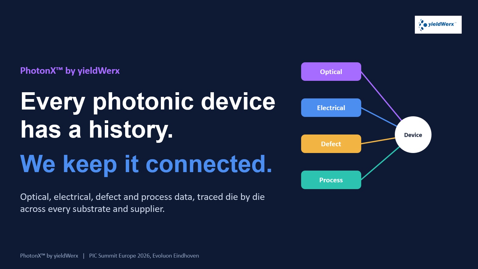
yieldWerx’s PhotonX™ traces photonic module failures back to the die. A photonic module can pass wafer-level tests and still fail after assembly or burn-in. When it does, the evidence may sit with several suppliers, each using its own identifiers and test records.
In a presentation prepared for PIC Summit Europe 2026, yieldWerx introduced yieldWerxIQ™ PhotonX™, a manufacturing analytics platform that links optical, electrical, defect and process data to the individual dies inside a finished module. The aim is to help engineers determine where a problem started, even if it only became visible several manufacturing steps later.
The presentation illustrates the problem with a module that combines a silicon photonics die, a compound-semiconductor laser, a CMOS electronics die, an interposer and a fiber attachment. Those elements can come from different suppliers or assembly operations. A weak optical signal at final test could reflect a problem with the laser, variation in the photonic circuit or misalignment during fiber attachment. The final reading shows the symptom. Tracing the parts and measurements through assembly gives engineers a way to distinguish among those possibilities.
PhotonX™ uses the platform’s intelligence module, DataIQ™ to build what yieldWerx calls a manufacturing genealogy. A measurement stays attached to the stage where it was taken, whether that is a lot, a wafer, a die at a specific wafer coordinate, a bonded stack or a finished module. The record can bring together optical spectra and insertion loss measurements, electrical test results, inspection maps and process records. Engineers can then compare what they saw at final test with what was measured before the components were bonded. yieldwerx.com
The new yieldWerx IQ™ platform consists of multiple intelligence modules that assists the manufacturing process during different phases in the lifecycle. APATIQ™ screens for unusual combinations of optical and electrical readings, even when each measurement falls within its individual limit. SignatureIQ™ identifies spatial patterns, such as an edge ring on a wafer that could point to a process issue. DefectIQ™ overlays inline inspection results with optical and electrical measurements at the same die coordinates. The presentation says teams can run rules in monitor-only mode, so they can see which devices a rule would flag before letting it affect production decisions.
Packaging changes the economics of a missed defect. By the time a module fails, a manufacturer may have bonded several dies, attached fibers and spent time on test and burn-in. A screening rule that reliably identifies risky dies earlier could avoid spending those resources on modules likely to fail. But a rule that flags too many good dies can also cut yield. Linked wafer and module records let teams look back at both groups and check whether a proposed screen would have caught failures without discarding too many usable parts.
Co-packaged optics makes that trade-off especially important. When photonic and electronic dies sit alongside a high-value ASIC in the same package, a problem in one component can put the entire assembly at risk. If engineers can tie module-level bit error rates to earlier optical or electrical measurements, they can test whether the best intervention is a tighter wafer screen, a process change or an adjustment during assembly. That distinction matters because each fix falls to a different team and may involve a different supplier.
Bottom line: The presentation uses illustrative data to show how multivariate screening works. Its production value will depend on how consistently manufacturers can preserve die identity across handoffs and how well the signals hold up across lots, suppliers and assembly conditions. A wafer pattern can give engineers a place to look, and an outlier score can identify a part to investigate. The stronger test is whether either signal predicts failures on later lots and whether acting on it improves finished-module yield. That is the link PhotonX™ is designed to make measurable, from wafer test through final assembly.
Also Read:
Technical Case Study: MicroLED Yield Management with Plessey and yieldWerx
yieldWerx Delivers a Master Class in Co-Packaged Photonics Implementation
CEO Interview with Aftkhar Aslam of yieldWerx
Share this post via:


Comments
There are no comments yet.
You must register or log in to view/post comments.