





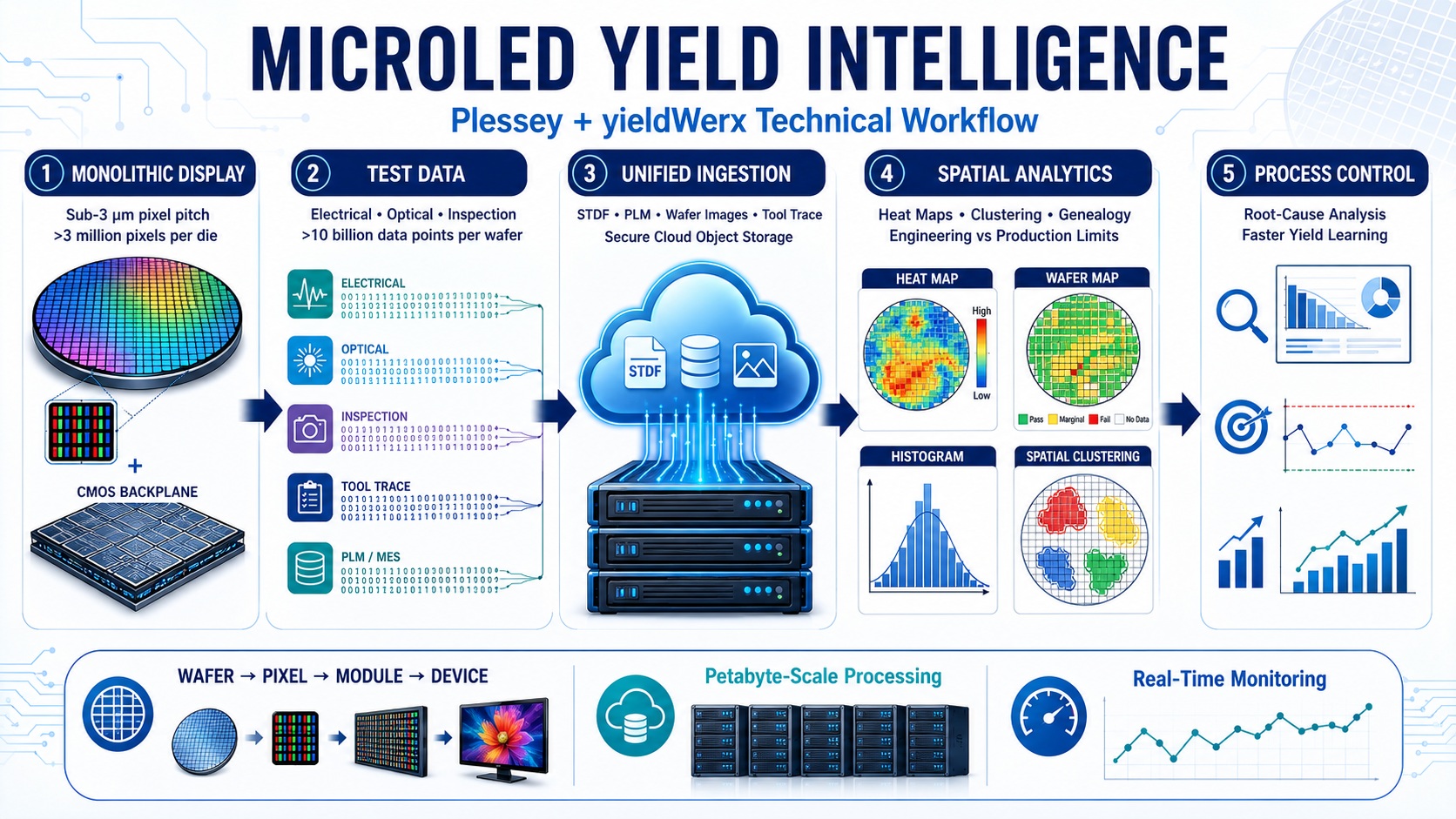
Plessey Semiconductors manufactures monolithic MicroLED displays for near-eye augmented-reality systems, where pixel pitch, brightness, uniformity, and defect density directly determine usable yield. Its process integrates device design, epitaxy, wafer fabrication, bonding, and production in one facility. The displays use sub-3-micrometre pixel geometries and can generate luminance of several million nits. A die contains more than three million pixels, while a wafer may contain billions. Because every pixel produces several optical and electrical measurements, a single wafer can generate more than ten billion data points.
This density creates failure mechanisms and analytical loads that conventional semiconductor yield systems were not designed to handle. A microscopic particle or small alignment error can affect millions of pixels on the CMOS backplane. Pixel-rich MicroLED wafers may produce between ten and one thousand times more test data than conventional monolithic devices, overwhelming legacy databases. Wafer-level fusion bonding adds another challenge: engineers must preserve genealogy between the MicroLED array and the incoming CMOS substrate so that downstream failures can be traced to the correct material, process step, or tool. Fixed pass/fail limits are also unsuitable during development, when engineers need to inspect marginal dies without changing qualified production criteria.
Plessey deployed yieldWerx as a centralized yield-management and analytics platform. The system ingests heterogeneous test and inspection streams, structures them in a common repository, and connects wafer-level results with pixel-level measurements. General electrical and array-optical data are imported through Standard Test Data Format files. Electrical parameters include continuity, leakage, power, and functional status. Optical parameters include average display luminance in raw, scaled, or normalized form; peak and dominant wavelength; full width at half maximum; centroid values; and test images.
High-resolution spatial analysis correlates inline defect-inspection records with electrical measurements. Spatial clustering separates isolated random defects from systematic signatures such as contamination, alignment drift, or process nonuniformity. This distinction is important because random events may require localized screening, whereas repeated spatial patterns can indicate correctable equipment or process conditions. The architecture is also transitioning toward distributed, secure cloud-object storage to support high-throughput ingestion and petabyte-scale processing.
Cross-domain integration maintains the relationship between both substrates through fusion bonding. By linking incoming-wafer inspection, inline defectivity, end-of-line electrical results, and pixel-level optical performance, engineers can navigate from wafer to pixel, module, and finished device. This genealogy shortens root-cause analysis and strengthens manufacturing and supply-chain traceability.
For pixel-level analysis, yieldWerx ingests complete luminance maps of active displays, described as stitched pixel-level measurements. It also analyzes checkerboard and inverse-checkerboard patterns, which compare energized and non-energized regions, and calculates luminance uniformity across the active area. Engineers can examine these measurements using gradient, grayscale, or pass/fail heat maps, together with histograms, box plots, trend charts, and wafer maps assembled from test images. These views expose local defects, distribution tails, spatial gradients, and wafer-to-wafer drift that summary yield percentages could conceal.
A dual-mode threshold configuration separates exploratory engineering limits from controlled production limits. Interactive settings for dim and dead pixels allow development teams to study sensitivity and optimize binning without modifying released manufacturing rules. This supports new-product introduction while protecting production consistency.
The implementation establishes a technical foundation for real-time monitoring, automated outlier detection, scalable defect classification, and pixel-resolution limits management. Importantly, the case study describes cloud migration and evaluation across production lots as ongoing activities, so anticipated benefits should not be interpreted as completed, quantified yield gains. The expected operational effects are faster yield learning, improved engineering velocity, greater yield stability, lower infrastructure and cost-per-pixel burdens, stronger quality control, and shorter time to market. For monolithic AR displays, the central achievement is not merely storing more measurements; it is preserving context across vast, heterogeneous datasets so engineers can convert pixel-scale evidence into timely wafer-scale process decisions. That capability is valuable in MicroLED manufacturing, where aggregate die classifications alone cannot reveal whether brightness loss, wavelength variation, leakage, or dead pixels share a common spatial origin. Unified analytics therefore connects device physics, process control, and production economics.
You can find the source material HERE.
Also Read:
yieldWerx Delivers a Master Class in Co-Packaged Photonics Implementation
WEBINAR: Outrunning the Data Wave – Why we need to keep pace with the coming 400% data surge
CEO Interview with Aftkhar Aslam of yieldWerx
Share this post via:



Comments
There are no comments yet.
You must register or log in to view/post comments.