





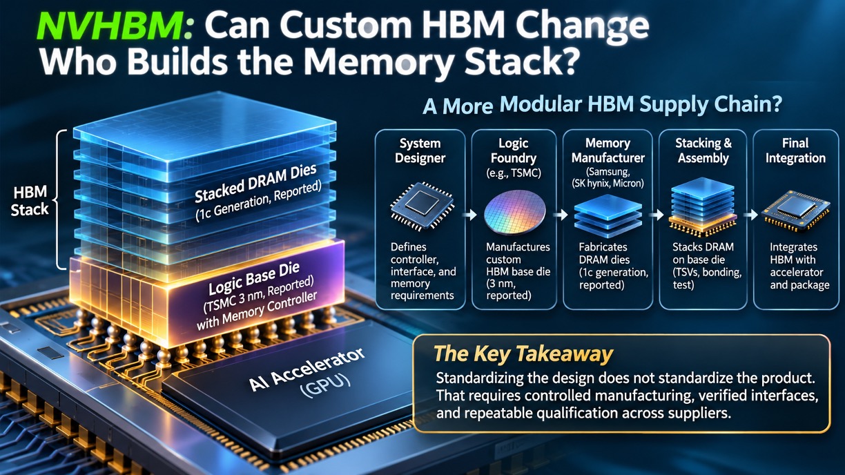
NVIDIA’s NVHBM could change more than how memory connects to an AI accelerator. It could also change how the semiconductor industry divides responsibility for designing, manufacturing, and qualifying high-bandwidth memory.
According to October 18 reporting from Seoul Economic Daily, NVIDIA has asked Samsung, SK hynix, and Micron to use TSMC’s 3 nm process for NVHBM logic base dies. The report also describes a request to standardize the DRAM dies around the sixth-generation 1c process generation.
Samsung reportedly accepted the requirements, despite traditionally relying on its own foundry operations for HBM production. These arrangements remain industry reporting rather than a publicly confirmed manufacturing agreement among the companies.
The distinction is important. NVIDIA is not proposing to manufacture the entire memory stack using a 3 nm logic process. The base die and stacked DRAM dies perform different functions and require different manufacturing technologies.
But the reported direction raises a larger engineering question:
If the system designer defines the memory architecture, a foundry manufactures the logic base die, and memory suppliers fabricate and stack the DRAM, could HBM become a more modular manufacturing product?
The answer depends on much more than using the same semiconductor process.
1. What Is Changing?
Conventional HBM combines vertically stacked DRAM dies with a logic base die. The DRAM provides memory capacity, while the base die manages supporting functions and the physical interface to the processor. The memory controller typically resides on the accelerator.
NVHBM changes this partitioning by integrating NVIDIA’s custom memory controller into the HBM base die and redesigning the interface between memory and compute.
This makes the base die a more significant architectural component and creates an opportunity to separate its fabrication from the specialized processes used to manufacture DRAM.
The direction is not entirely new.
In April 2024, SK hynix announced a collaboration with TSMC to apply advanced foundry technology to HBM4 base dies. In December 2024, Marvell introduced a custom HBM architecture combining base-die logic, controller functionality, advanced die-to-die interfaces, and packaging.
NVIDIA’s approach extends this trend by pursuing a common custom architecture across multiple memory suppliers.
The reported 1c DRAM requirement adds another dimension. Rather than standardizing only the logic base die, NVIDIA appears to be seeking greater consistency in the underlying DRAM technology generation.
However, using the same DRAM generation does not mean different manufacturers employ identical processes, device structures, or manufacturing flows.
The architectural shift is toward defining memory requirements across companies while allowing specialized manufacturers to execute different parts of the product.
2. What Could Become More Modular?
HBM has traditionally been delivered as a tightly integrated memory product.
DRAM fabrication, TSV formation, wafer thinning, die stacking, bonding, testing, and qualification must operate as a coordinated manufacturing process.
A standardized custom base die could create a clearer division of responsibilities:
- System designer: Defines the controller, memory interface, and system-level performance requirements.
- Logic foundry: Manufactures the customized base die using an advanced logic process.
- Memory manufacturer: Produces DRAM dies and integrates them into a completed memory stack.
- Advanced packaging provider: Integrates the qualified memory stacks with the accelerator and package interconnect.
This division already exists in various forms. What changes is the potential for greater standardization across participating suppliers.
If the processor-facing interface and controller architecture are common, system designers may be able to reduce certain differences between memory implementations.
But there is an important limit.
A common architecture does not automatically produce interchangeable memory stacks.
Two suppliers using the same base-die process and DRAM technology generation can still produce devices with different operating margins, thermal characteristics, power consumption, manufacturing variation, and reliability.
A standardized design creates the possibility of modular manufacturing. It does not establish manufacturing equivalence.
3. Where Do the Manufacturing Challenges Move?
Separating the base die from DRAM fabrication does not eliminate HBM’s physical complexity.
The completed stack still requires high-density vertical interconnects, precise die alignment, bonding integrity, controlled power delivery, thermal management, and extensive testing.
In fact, separating manufacturing responsibilities makes several integration boundaries more important.
Base-die-to-DRAM integration
A logic die manufactured in one process must connect reliably to DRAM dies fabricated using another. The interface must accommodate differences in electrical characteristics, physical geometry, power requirements, and thermal behavior.
Stacking and bonding yield
HBM depends on reliable vertical connections through multiple DRAM layers. TSVs, bonding structures, alignment accuracy, and accumulated manufacturing variation remain central to final product yield.
A qualified base die and individually tested DRAM dies do not guarantee a high-yield completed stack.
Thermal and power behavior
Moving controller functionality into the base die changes where power is dissipated. The thermal design must consider logic activity, heat transfer through the DRAM stack, and the operating environment created by the neighboring accelerator.
Test access and failure isolation
When different companies manufacture the base die and DRAM, test strategies must identify where failures originate.
A failure observed at the package level could involve the DRAM array, controller logic, vertical interconnect, bonding process, power delivery, or surrounding package.
That requires effective intermediate testing, diagnostic visibility, and traceability across manufacturing steps.
Qualification and reliability
The final product must demonstrate acceptable bandwidth, latency, power, thermal performance, and long-term reliability under representative operating conditions.
Standardizing the process technology may reduce some sources of variation, but it does not remove the need to qualify each supplier’s finished memory product.
This is where the proposed modularity faces its most demanding test.
4. Could This Change Who Manufactures HBM?
Potentially, although the distinction between supplying memory components and delivering a qualified HBM stack remains substantial.
Separating base-die manufacturing from DRAM fabrication could allow companies to specialize more deeply in particular stages of the manufacturing flow.
An advanced logic foundry could fabricate controller-equipped base dies. A memory manufacturer could focus on competitive DRAM technology and high-density stacking. A specialized assembly provider could potentially perform selected integration and test activities.
But that final arrangement is a possible future manufacturing model, not an established consequence of NVIDIA’s reported requirements.
A company entering this supply chain would still need access to competitive DRAM technology, qualified stacking and bonding processes, known-good-die strategies, thermal characterization, failure analysis, and product qualification capabilities.
Economics also matters.
Splitting manufacturing across organizations introduces logistics, intermediate testing, traceability, yield ownership, and coordination costs.
A modular manufacturing flow succeeds only if the resulting flexibility and specialization compensate for those additional requirements.
Existing HBM manufacturers would also retain significant technical differentiation through DRAM cell density, power efficiency, stacking capability, process control, and yield.
The opportunity is therefore not simply to replace vertically integrated memory manufacturing.
It is to determine which manufacturing activities benefit from specialization and which must remain tightly coupled to protect yield, performance, and reliability.
5. What Would Prove That the Model Works?
The critical milestone would not be the announcement of a shared base-die process.
It would be demonstrating that multiple suppliers can repeatedly deliver complete memory stacks meeting common system requirements.
That requires more than matching nominal specifications.
Engineers would need to compare actual products across several dimensions: bandwidth, latency, power consumption, signal integrity, thermal behavior, manufacturing variation, and reliability.
They would need to establish appropriate test coverage before and after stacking, correlate electrical performance with physical manufacturing variation, and identify which processes control the most important performance and yield margins.
They would also need clear responsibilities for failure analysis and corrective action when problems cross organizational boundaries.
Consider two suppliers using the same NVIDIA-defined base-die architecture.
Both might meet the required bandwidth under nominal conditions. But differences in DRAM characteristics, bonding quality, thermal resistance, or assembly variation could produce different operating margins.
Those differences may not become visible until temperature, voltage, workload, or aging conditions change.
The products share an architecture, but their manufacturing outcomes are not necessarily equivalent.
The true measure of standardization is not whether suppliers can manufacture the same design. It is whether they can repeatedly deliver products that satisfy the same qualified operating requirements.
That distinction determines whether modular manufacturing delivers practical flexibility or merely creates additional interfaces to manage.
The Engineering Takeaway
NVHBM illustrates a broader direction in semiconductor integration: architectural ownership and manufacturing ownership do not necessarily have to reside within the same company.
The system designer can define more of the memory architecture. An advanced foundry can manufacture the logic base die. Memory suppliers can apply their expertise in DRAM fabrication and stacking. Packaging providers can integrate those components into complete accelerator systems.
But separating these responsibilities does not eliminate the physical dependencies between them.
It increases the importance of interface definitions, process control, test coverage, manufacturing traceability, and qualification.
The reported TSMC 3 nm and 1c DRAM requirements are therefore interesting not simply because they could align manufacturing technologies across suppliers, but because they raise the possibility of a more standardized manufacturing ecosystem.
Whether that ecosystem becomes genuinely modular will depend on demonstrated product-level results.
Moh’s Golden Rule: Standardizing the design does not standardize the product. That requires controlled manufacturing, verified interfaces, and repeatable qualification across suppliers.
The next transformation in HBM may not be only how memory is designed, but how reliably the industry can manufacture it across organizational boundaries.
References
- NVIDIA, NVIDIA NVLink Fusion Brings NVHBM to Next-Generation AI Infrastructure, August 26, 2026.
https://developer.nvidia.com/blog/?p=120848 - Seoul Economic Daily, Samsung to Tap TSMC for Nvidia’s Custom HBM Base Die, October 18, 2026.
https://dcb0ucee30q2g.cloudfront.net/finance/2026/10/18/samsung-to-use-tsmc-for-base-die-in-nvidias-custom-hbm - Reuters, Samsung to use TSMC technology for Nvidia’s next-generation memory chips, Seoul newspaper reports, October 18, 2026.
https://www.reuters.com/world/asia-pacific/samsung-use-tsmc-technology-nvidias-next-generation-memory-chips-seoul-newspaper-2026-10-18/ - SK hynix, SK hynix Partners with TSMC to Strengthen HBM Technological Leadership, April 19, 2024.
https://news.skhynix.com/en/sk-hynix-partners-with-tsmc-to-strengthen-hbm-technological-leadership/ - Marvell, Marvell Announces Breakthrough Custom HBM Compute Architecture to Optimize Cloud AI Accelerators, December 10, 2024.
https://www.marvell.com/company/newsroom/marvell-announces-breakthrough-custom-hbm-compute-architecture.html
Also Read:
Who Owns the Voice in Your Head?
Intel’s Tiny Bridges Could Lead to Very Big Paychecks
High-NA’s Obituary Was Premature
Share this post via:


The $725 Million Chip Development: Why Execution Risk, Not IP Cost, Now Dictates Advanced-Node Survival