

Agentic AI Can Reach GDS. What Must It Prove Before Engineers Trust It for Tapeout?

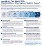
Agentic AI Can Reach GDS. What Must It Prove Before Engineers Trust It for Tapeout?
by Moh Kolb on 09-29-2026 at 6:00 am

AgentiC AI SemiWIKI sept21

Agentic AI is beginning to move semiconductor engineering beyond copilots and isolated task automation.

From Agentrys’ public material and recent discussion, its architecture points toward a broader engineering flow:

Specification → RTL → verification → synthesis / physical design → PPA optimization → physical verification… Read More


The Future of CPO May Be a Glass Integration Platform

The Future of CPO May Be a Glass Integration Platform
by Moh Kolb on 09-21-2026 at 8:00 am

CPO on a glass patfrom

Co-packaged optics is usually described as a proximity problem.

Move the optical engine closer to the switch ASIC or XPU. Shorten the electrical path. Reduce SerDes power. Increase bandwidth density.

That direction is real.

Optical functionality is moving progressively closer to compute.

But proximity does not eliminate … Read More


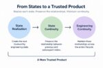
Semiconductor Engineering Has a State-Continuity Problem

Semiconductor Engineering Has a State-Continuity Problem
by Moh Kolb on 09-14-2026 at 8:00 am

Semi eng state conti Problem sept11 semiwiki

Product realization depends not only on reaching the next engineering state, but on preserving the relationships between states from intent through qualification, release, and lifecycle learning.

Semiconductor development is usually described as a sequence of activities: architecture, design, fabrication, packaging,… Read More


When Design Gets Faster, the Bottleneck Moves Through the Physical Stack

When Design Gets Faster, the Bottleneck Moves Through the Physical Stack
by Moh Kolb on 09-07-2026 at 6:00 am

Desing fast Bott through physicalstack

AI can compress the path to tape-out. The next challenge is compressing physical realization.

Something important is beginning to happen in semiconductor development: the design cycle itself is becoming compressible.

AI-assisted engineering can accelerate architecture exploration, RTL development, verification, physical… Read More


The Fab Is Not the Finish Line

The Fab Is Not the Finish Line
by Moh Kolb on 08-20-2026 at 6:00 am

FAb is not the finish line (1)

AI may close the design. The fab may finish the silicon. Production still has to realize the system.

Semiconductor engineering is becoming extraordinarily capable.

EDA platforms are expanding from individual design tasks toward increasingly complete system analysis.

Multiphysics simulation is connecting electrical, … Read More


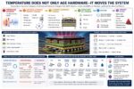
Temperature Does Not Only Age Hardware — It Moves the System

Temperature Does Not Only Age Hardware — It Moves the System
by Moh Kolb on 08-11-2026 at 2:00 pm

Temp not age HW Moves ys semiAug2

Temperature is often treated as a reliability clock.

Increase the temperature, accelerate the failure mechanism, and estimate the equivalent field life.

That approach can be useful—but only when the dominant failure mechanism is known, its thermal activation behavior is understood, and the same mechanism remains active … Read More


From Photonics Precision to Repeatable Evidence

From Photonics Precision to Repeatable Evidence
by Moh Kolb on 07-30-2026 at 2:00 pm

Photroinc probe july112 semi

Why Optical Probing Is Becoming a Manufacturing Boundary for Silicon Photonics

Silicon photonics has already shown that extremely precise optical alignment is possible.

In controlled laboratory environments, engineers can align fibers, waveguides, grating couplers, edge couplers, modulators, detectors, and electrical… Read More


The Packaging PDK Is the Missing Layer for Co-Packaged Optics

The Packaging PDK Is the Missing Layer for Co-Packaged Optics
by Moh Kolb on 07-07-2026 at 10:00 am

PKG PDK MISSION CPO JUne26

From Photonic Device Design to Electro-Optical Realization

Co-packaged optics will not scale through photonic device performance alone.

As AI infrastructure pushes bandwidth, power, latency, and reach to new limits, optics is moving closer to the compute engine. The industry is no longer asking only whether a photonic device… Read More


The Modulator Is Not the Product: Why AI Photonics Needs an Electro-Optical Realization Corridor

The Modulator Is Not the Product: Why AI Photonics Needs an Electro-Optical Realization Corridor
by Moh Kolb on 06-24-2026 at 10:00 am

Picture BORB EORC June19

Co-packaged optics, silicon photonics, optical I/O, and photonic engines are becoming central topics in the future of AI infrastructure.

The common story is simple:

Copper is reaching limits.
Light can move data farther and more efficiently.
Therefore, AI systems will move from electrical interconnects toward optical interconnects.… Read More


A tower-like heterogeneous packaging architecture for the AI era

A tower-like heterogeneous packaging architecture for the AI era
by Moh Kolb on 06-16-2026 at 6:00 am

Picture1 VTEMC

For years, advanced packaging has been described mostly in planar terms: chiplets placed side by side, connected through interposers, bridges, redistribution layers, substrates, and short-reach electrical links. This view remains important. It supports today’s GPU, HBM, chiplet, and 2.5D integration architectures.… Read More