





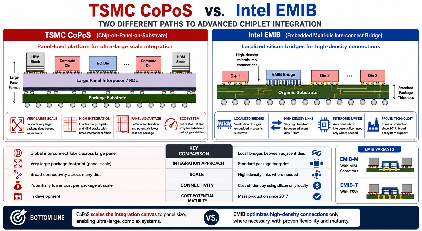
TSMC’s CoPoS, generally described as Chip-on-Panel-on-Substrate, and Intel’s EMIB, or Embedded Multi-die Interconnect Bridge, address the same strategic problem: integrating increasingly large, heterogeneous chiplet systems. However, they attack different physical constraints. CoPoS is an emerging panel-level packaging platform intended to extend interposer scale and manufacturing productivity beyond round wafers. EMIB is a production-proven localized silicon-bridge architecture that removes the need for a full-size silicon interposer. TSMC has confirmed that CoPoS is under development, although detailed public specifications remain limited.
In CoPoS, redistribution structures and chip-integration processes are performed on a large rectangular panel rather than a circular silicon wafer. The rectangular format can improve area utilization because packages tile more efficiently, reducing unused edge area. More importantly, panel dimensions can support package footprints beyond practical wafer and reticle-derived limits. This makes CoPoS attractive for future AI accelerators combining multiple compute dies, I/O dies, and numerous high-bandwidth-memory stacks. Nevertheless, interconnect pitches, qualified materials, yields, reliability data, and production schedules are less publicly defined than those of TSMC’s established CoWoS platform.
EMIB uses small silicon bridge dies embedded locally inside an organic package substrate. Fine-pitch microbumps connect adjacent chiplets to high-density wiring within each bridge, while conventional substrate routing handles lower-density signals and power elsewhere. Because silicon is placed only where dense die-to-die communication is required, EMIB avoids the area, cost, and through-interposer routing burden of a monolithic silicon interposer. Intel positions EMIB for logic-to-logic and logic-to-HBM connections and reports that the technology has supported mass production since 2017.
The primary architectural distinction is global versus local integration. CoPoS is best understood as a manufacturing and scaling framework for constructing very large interposer or redistribution-layer assemblies across a panel. It can provide broad routing connectivity among many dies and memory stacks, resembling a larger-format evolution of wafer-level 2.5D integration. EMIB instead creates point-to-point shoreline links between neighboring dies. This modularity lets designers deploy multiple bridges with link-specific routing while preserving much of the organic substrate for conventional power and external I/O distribution.
These choices produce different electrical trade-offs. A broad CoPoS redistribution fabric could simplify complex multi-die topologies and support extensive fan-out, but long global routes may introduce resistance, capacitance, latency, and signal-integrity challenges. Panel warpage, lithographic uniformity, overlay accuracy, and fine-line yield across a large rectangular area are also central process risks. EMIB minimizes high-density silicon routing length and does not force unrelated power or signals through a full interposer. However, its localized geometry requires careful chiplet placement, bridge alignment, escape routing, and die-edge bandwidth planning. Communication between nonadjacent dies may require additional bridges or package-level hops.
Thermally, neither technology eliminates the difficulty of cooling tightly packed AI silicon and HBM. CoPoS may enable extremely large assemblies, increasing total package power, mechanical stress, and cooling complexity. EMIB’s absence of a full silicon interposer can reduce some structural and routing constraints, but high-power chiplets still require advanced heat spreaders, substrate engineering, and power delivery. Intel’s EMIB-M incorporates metal-insulator-metal capacitors, while EMIB-T adds through-silicon vias to strengthen power delivery and support HBM-oriented configurations.
Ecosystem compatibility also differs today: CoPoS will likely benefit customers already using TSMC’s 3DFabric design flows, foundry nodes, and HBM assembly ecosystem, whereas EMIB integrates dies from Intel or external foundries and can be combined with Foveros stacking to create more complex 3.5D systems.
Manufacturing maturity is currently EMIB’s clearest advantage. Its product history provides validated assembly flows, reliability experience, and established design methodology. CoPoS offers potentially greater package-scale economics and geometric freedom, but panel-level semiconductor packaging must achieve wafer-like overlay, cleanliness, defect control, and yield before competing broadly.
Bottom line: CoPoS and EMIB are not direct substitutes. CoPoS targets the scaling of the integration canvas; EMIB optimizes where high-density connections are physically necessary. For near-term heterogeneous products requiring proven, flexible local interconnects, EMIB is lower risk. For future ultra-large AI systems constrained by wafer-format area and throughput, CoPoS could provide a more expansive platform—provided TSMC converts panel-level scale into acceptable interconnect density, warpage control, reliability, and cost.
Also Read:
TSMC CoWoS versus Intel EMIB Semiconductor Packaging
TSMC A16 Backside Power at VLSI 2026
Foundation IP for Intel 18A: Technical Overview and Why It Matters
Share this post via:



Comments
2 Replies to “TSMC CoPoS Versus Intel EMIB Semiconductor Packaging”
You must register or log in to view/post comments.