





Intel Foundry has a blog on LinkedIn that is worth a look. The blogs are by trusted Intel Foundry technical experts and are filled with content. I will cherry pick write a bit about them but be sure and subscribe to this, absolutely.
Intel 18A-P is not a new process node in the conventional sense. It is a performance-enhanced derivative of Intel 18A designed to provide higher transistor drive, lower interconnect resistance and improved thermal behavior without forcing customers to rebuild their designs around a different technology platform. Intel reports more than 9% higher performance at constant power or over 18% lower power at constant performance, based on measurements from an Arm processor-core sub-block.
The foundation remains Intel 18A’s combination of RibbonFET gate-all-around transistors and PowerVia backside power delivery. RibbonFET surrounds the transistor channel with the gate, improving electrostatic control as dimensions shrink. PowerVia relocates the power-distribution network from the signal-routing side of the wafer to its backside. Separating power and signal wiring reduces frontside congestion, lowers power-delivery impedance and gives design tools more freedom when routing timing-critical nets.
Intel 18A-P extracts additional performance from this architecture through device, contact and interconnect optimization. Its expanded transistor portfolio includes low-capacitance W1 and W1.5 devices for power-sensitive logic and a high-performance W3P device incorporating Power Boost. This broader menu allows implementation tools to select transistors according to the timing, leakage and switching-energy requirements of individual paths rather than applying one aggressive device configuration throughout a block.
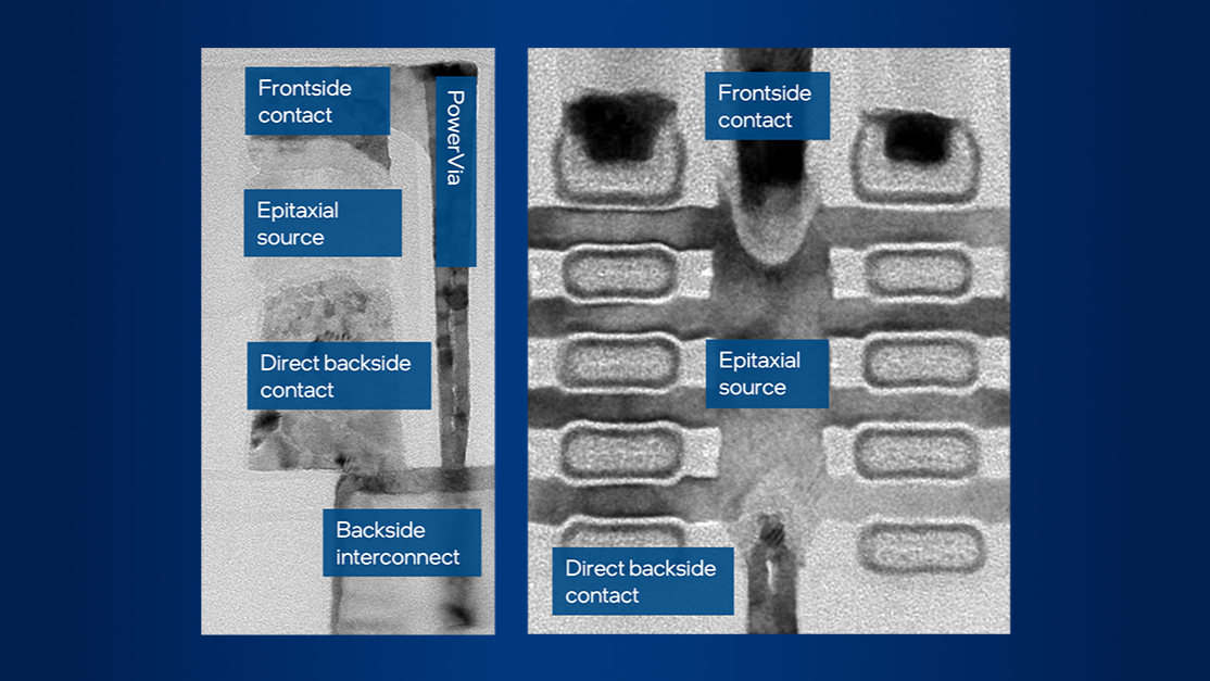
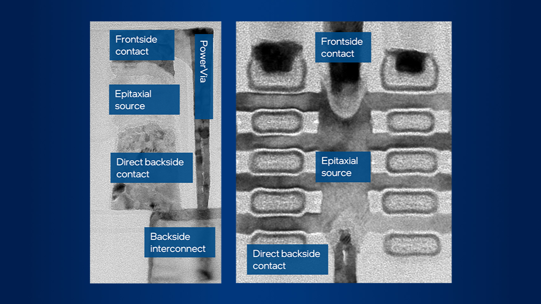
Power Boost is the most distinctive enhancement. It employs a dual-contact structure that combines a conventional frontside contact with a direct backside connection enabled by PowerVia. The objective is to reduce external resistance between the transistor and power network without increasing the transistor footprint or its switched capacitance. Intel reports approximately 20% lower external resistance for NMOS devices and 12% for PMOS devices. The resulting improvement in delivered current allows W3P transistors to operate more than 10% faster at matched capacitance.
Strain engineering provides another important contribution, particularly for PMOS performance. Carefully controlled mechanical stress changes carrier mobility within the channel, increasing current without simply enlarging the device. Intel reports approximately 5% higher NMOS drive current and 16% higher PMOS drive current relative to Intel 18A. Together with lower contact resistance, these improvements produce an estimated 12% increase in circuit-level switching speed.
The interconnect stack has also been refined. Via resistance falls by roughly 10% to 30% in performance-critical layers, while optimized metal jogs reduce routing inefficiencies. These changes matter because advanced-node performance is increasingly limited by wiring and contact parasitics rather than transistor switching alone. A faster device provides little system benefit if resistive vias and heavily loaded routes consume the recovered timing margin.
Intel 18A-P also introduces another intermediate threshold-voltage pair and approximately 33% tighter skew corners. More threshold options give synthesis and place-and-route systems finer control over the trade-off between leakage and delay. Tighter process corners reduce uncertainty between fast and slow device populations, potentially allowing designers to recover margin that would otherwise be reserved for manufacturing variation.
Compatibility may be as commercially significant as the raw performance. Intel Foundry says Intel 18A-P retains Intel 18A design rules, SRAM offerings, minimum SRAM operating voltage, IP and design infrastructure. Customers can therefore migrate existing blocks without the disruption normally associated with a full-node transition. Reusing libraries, memories, verification flows and physical-design methodology lowers engineering cost and reduces schedule risk.
Thermal improvements address sustained performance rather than benchmark frequency alone. Material and bonding-stack changes increase bond-stack thermal conductance by 50%, according to Intel Foundry, contributing to a claimed 20% to 40% reduction in overall stack thermal resistance. That can reduce thermal throttling in continuously utilized AI accelerators and data-center processors, although realized benefits will depend on packaging, cooling and system design.
Reliability remains critical because higher current density and backside processing can introduce new failure mechanisms. Intel Foundry reports improved PMOS negative-bias temperature-instability behavior while maintaining Intel 18A targets for gate-oxide and hot-carrier reliability.
Technically, Intel 18A-P illustrates how process advancement is changing. Meaningful gains increasingly come from coordinated optimization across transistors, contacts, interconnects, power delivery, thermal structures and EDA flows. Its success will ultimately depend on production yield and customer silicon, but the architecture offers a credible route to better power-performance efficiency without discarding existing Intel 18A investments.
You can read the full article here.
And for entertainment:
Also Read:
Intel’s 14A Is Winning the Race Against Defects
Crescent Island: Turning Memory Capacity into Agentic AI Throughput
Intel Diamond Rapids: Building Xeon Up, Out, and Through Silicon
Share this post via:



Comments
5 Replies to “Intel 18A-P Pushes RibbonFET and Backside Power Beyond the First Generation”
You must register or log in to view/post comments.