







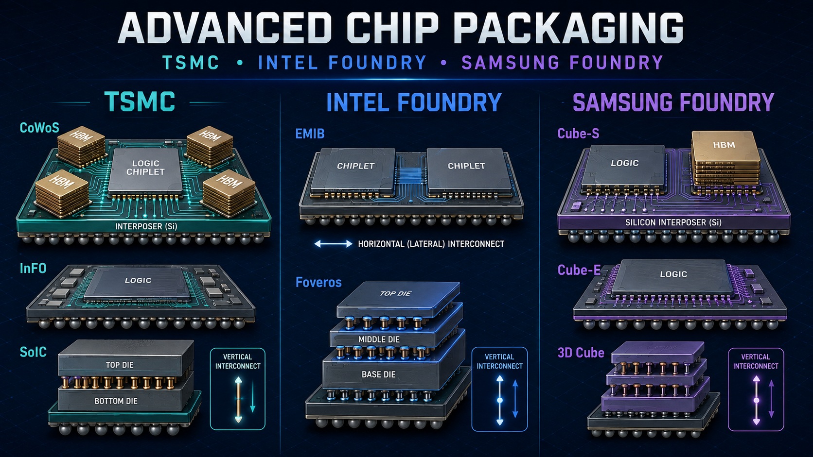
Advanced semiconductor packaging has become essential to improving computing performance as conventional transistor scaling grows more difficult and expensive. Instead of manufacturing an entire processor as one large monolithic die, chipmakers can divide it into smaller chiplets and combine logic, memory, input/output and specialized accelerators within one package. TSMC, Intel Foundry and Samsung Foundry all offer technologies for this purpose, but their portfolios differ in architecture, maturity, market position and integration strategy.
TSMC groups its advanced packaging technologies under the 3DFabric platform. Its principal offerings are CoWoS, InFO and SoIC. CoWoS, or Chip-on-Wafer-on-Substrate, is primarily a 2.5D technology for high-performance computing and artificial intelligence. It places logic dies and high-bandwidth memory, or HBM, on an interposer that provides dense, high-speed connections. CoWoS-S uses a silicon interposer, while CoWoS-L combines local silicon interconnects with a redistribution-layer structure. CoWoS-R relies more extensively on redistribution layers to provide a cost-conscious option for suitable designs.
CoWoS has become especially important for large AI accelerators, where several HBM stacks must communicate with GPUs or custom processors at enormous bandwidth. TSMC says CoWoS-S supports silicon interposers up to approximately 3.3 times the lithographic reticle size, while CoWoS-L and CoWoS-R address larger configurations. TSMC’s InFO family provides fan-out packaging without a conventional silicon interposer and is used where thin profiles, efficient wiring and lower cost are priorities. SoIC addresses true three-dimensional integration by directly stacking dies with dense vertical connections. SoIC stacks can also be incorporated into CoWoS or InFO packages, creating what TSMC calls a “3Dx3D” system. TSMC 3DFabric overview
Intel Foundry’s portfolio centers on EMIB and Foveros. EMIB, or Embedded Multi-die Interconnect Bridge, connects chiplets positioned side by side through small silicon bridges embedded in the organic package substrate. Unlike a full silicon interposer, EMIB places silicon only where dense die-to-die communication is needed. This can reduce silicon usage, simplify some aspects of assembly and allow designers to construct packages larger than a single reticle. EMIB is well suited to connecting compute tiles, I/O dies and HBM while leaving each component relatively accessible for cooling.
Foveros complements EMIB by supporting vertical integration. In a Foveros package, compute chiplets can be stacked on an active base die that provides communication or other functions. Foveros Direct uses copper-to-copper hybrid bonding to obtain finer connection pitches, lower resistance and greater bandwidth between stacked dies. Intel can combine Foveros stacks with EMIB bridges in an EMIB 3.5D package, gaining both vertical density and horizontal scalability. Intel is also expanding the portfolio with variants such as EMIB-T, which adds through-silicon vias, and Foveros-R, a redistribution-layer option intended to balance cost and performance. Intel Foundry packaging overview
Samsung Foundry offers comparable horizontal and vertical integration technologies. Its current horizontal portfolio includes 2.5D Cube-S and 2.3D Cube-E and Cube-R. Cube-S, previously associated with Samsung’s I-Cube naming, places logic chips and HBM on a silicon interposer. Samsung says qualified configurations can use a 3.3-reticle-size interposer and integrate up to eight HBM modules, with larger options supporting additional memory. Cube-E uses embedded silicon bridges, making it conceptually similar to Intel EMIB, while Cube-R employs a redistribution-layer interposer.
For vertical integration, Samsung offers 3D Cube technologies, formerly called X-Cube. The 3D Cube-T variant uses thermo-compression bonding in a chip-on-wafer process, while 3D Cube-H uses hybrid copper bonding for finer pitches and improved electrical performance. These technologies stack dies to shorten communication paths, save package area and reduce the yield risks associated with extremely large monolithic chips. Samsung’s broader strength is its ability to combine foundry manufacturing, packaging and memory expertise within one company—an attractive proposition for systems that depend heavily on HBM. Samsung Foundry packaging overview
Technically, the three companies are converging on similar categories. TSMC CoWoS-S and Samsung Cube-S use large silicon interposers for 2.5D integration. Intel EMIB and Samsung Cube-E use localized embedded bridges instead of full interposers. TSMC SoIC, Intel Foveros Direct and Samsung 3D Cube-H pursue dense vertical stacking through advanced bonding. Each vendor also offers redistribution-layer alternatives that can reduce cost where maximum silicon-interposer density is unnecessary.
Their main differences lie in execution and ecosystem. TSMC benefits from its position as the leading manufacturer of advanced chips for numerous fabless customers, giving 3DFabric and CoWoS a powerful customer base and extensive exposure to AI products. Intel brings long experience packaging its own complex processors and emphasizes flexible bridge-based integration, large package sizes and geographically distributed assembly capabilities. Samsung offers a vertically integrated route connecting logic fabrication, advanced packaging and memory production, although customers must evaluate its particular process maturity, design ecosystem, capacity and product requirements.
Bottom line: There is no universally superior portfolio. TSMC is especially prominent in interposer-based AI packaging; Intel differentiates itself through EMIB and combined 3.5D architectures; and Samsung offers a broad, increasingly unified set of interposer, bridge and vertical-stacking technologies. The correct choice depends on bandwidth, thermal limits, HBM count, chiplet sources, package size, production capacity, cost and supply-chain strategy.
Also Read:
Intel and TSMC Take Different Paths to High-NA EUV
Intel Foundry and the DAC2026 Ecosystem
Executive Interview with James Huang of AlChip
Share this post via:



Terafab’s Single Roof: Why Packaging, Not Lithography, Decides High Volume