


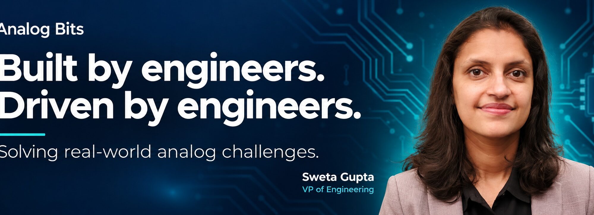


Sweta Gupta is the Vice President of Engineering at Analog Bits, where she leads development and execution of mixed-signal IP’s, managing circuit and layout teams.
Ms. Gupta has been a part of the Analog Bits team since 2004 and she has successfully managed and delivered high quality IP’s including low jitter PLL’s, low power crystal oscillators, PVT sensors, power supply monitors and power management IP’s on leading-edge process geometries. She received her MSEE degree from Arizona State University and BSEE degree from Osmania University, India.
What brought you to Analog Bits?
I joined Analog Bits in 2003, right after finishing my master’s in electrical engineering at Arizona State, as one of the company’s earliest employees. What drew me in was that this was a company built by engineers and driven by engineers, focused on solving real-world analog challenges. Twenty-plus years later, that is still how we operate.
As a hands-on circuit designer, I had the chance to work across every product the company had at the time. That breadth taught me how analog blocks interact in a real system, and it gave me room to grow. I went from designing circuits to managing projects in foundation analog IP, and eventually to leading our SerDes and power delivery product lines.
I’ve also watched the company itself evolve. We started with our roots in Silicon Valley and have grown into a global engineering organization spanning three continents, with teams in Silicon Valley, Prague, and South Korea. That footprint has changed how we work. Our engineers collaborate close to the customers and ecosystem foundry and EDA partners we serve, and the time zones give us a development rhythm that keeps design, characterization, and support moving around the clock. It also brings us different engineering perspectives, which makes the IP better in quality and assuring first time working silicon.
What I value most is how close engineering interacts with our customers especially in developing early product versions and future derivatives. I work not just with my team and peers but with applications engineering and directly with customers, because their requirements shape our roadmap. When a customer tells us what they need from a clock, a sensor, or a LDO at an advanced node, that input goes straight to the people designing the IP. That tight loop between customer needs and engineering decisions is a large part of how Analog Bits has evolved.
Bringing all of that collective experience together is our core strength, and I’m proud and honored to hold a leadership position as VP of Engineering.
What is the biggest challenge your customer is facing?
The biggest challenge our customers face today is managing power integrity, thermal runaway, and precise clocking at advanced sub-3nm nodes.
As massive AI workloads, multi-die chiplets, and high-density data centers push silicon to its physical limits, our customers’ advanced multicore SoCs are running into severe localized voltage droops caused by sudden current spikes, along with unpredictable thermal hotspots that threaten chip lifetime and performance. At the same time, processing enormous workloads across chiplet links and high-bandwidth interfaces demands extremely precise timing, where any clock jitter can ruin data integrity. Furthermore, taping out on leading-edge processes like TSMC N3P, N2P, or upcoming A14 represents a massive financial risk if the mixed-signal IP—from power management macros to high-frequency connectivity IPs—fails to behave predictably under extreme operating conditions.
Why is your approach to solving this problem unique?
Our uniqueness mostly comes from our ability to listen to the customer needs and create new product categories to solve the increasing demands for integration. This may sound cliched, but to illustrate, we may have made the most compact and power optimized wide-range PLL IP over 20 years ago to address the clocking needs at that time, but through continuous listening to and engagement with our customers, we are today creating numerous power monitoring and controlling IP to ease the power delivery issues that have become commonplace now in modern high power low-voltage chips.
Another unique aspect is that we don’t just validate in simulation and hand customers a datasheet. We validate in silicon, tape out our own test chips, populate them with our full portfolio of PLLs, SerDes, sensors, and power management IP, and characterize them across process, voltage, and temperature extremes, including noise and power-supply conditions that emulates a real SoC. We do this across TSMC, Samsung, Intel and GlobalFoundries, on FinFET and GAA nodes. We carry that risk before our customers have to, so what they integrate has already been measured on silicon at their node. That’s how we shorten their path to first-pass success.
What other approaches are being used to solve this problem?
Some SoC companies choose to develop critical IP in-house to maintain greater control, customization, and differentiation. However, developing and validating complex mixed-signal IP requires specialized engineering expertise, significant investment, and considerable time. This can divert resources from core product innovation, increase development costs, and extend time to market—particularly at advanced process nodes, where silicon validation and first-pass success are critical. What Analog Bits brings is the volume of customer experience and even the largest ASIC suppliers with internal analog team today views us as partners.
What challenges will your customers face in the near future?
Three things. First, energy-efficient compute. At advanced nodes, power delivery and power sensing decide how much performance a design can achieve reliably, so we’re investing in on-die sensors and telemetry that tell customers where power is used in real time. Second, 3D stacking and chiplets. Thermal problems compound when dies are stacked, so we’re pushing sensor accuracy and responsiveness to the physical limits. Chiplet designs also need to integrate external components, which is why we’re leading on pinless technology and integrated high-performance clocking, which reduce pin count and board-level dependencies. Third, edge devices, where the power budget is in milliwatts. There we optimize every microamp in our IP.
How has AI changed your business strategy?
AI changed who our customers are and how we work. Almost every advanced-node customer is building for AI, whether in data centers and HPC, at the edge, or in automotive, so our roadmap is shaped by their needs for power, thermal management, and high-speed clocking. Internally, we’re adopting AI across engineering, QA, and customer support, to speed up design iteration and verification and to scale what a team can cover. It’s a continuous adoption, and it’s how we scale Analog Bits to the next level.
Also Read:
Inside the Silicon: Analog Bits N2P2 Test Chip
Analog Bits Targets the Power Challenge at the Heart of Next-Generation Chips
What Winemakers and Chip Designers Have in Common
Share this post via:


Comments
There are no comments yet.
You must register or log in to view/post comments.