




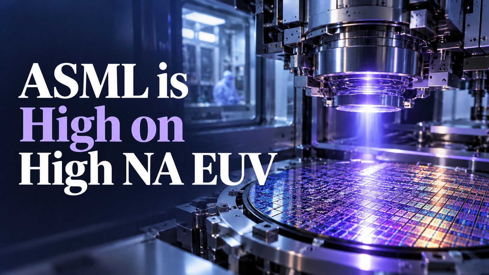

ASML’s grip on the most advanced corner of chip manufacturing is tightening. The Dutch company, already the sole supplier of extreme ultraviolet lithography systems, is winning broader industry support for High Numerical Aperture EUV, or High NA, its next-generation technology for printing smaller and denser circuitry.
That support matters because High NA machines cost roughly $400 million each, about twice as much as conventional EUV systems. Their adoption therefore depends on more than technical performance: chipmakers must believe the tools can improve yields, reduce production steps and remain useful across several generations of processors. Recent commitments from Intel, Samsung, TSMC and SK Hynix indicate that the industry is increasingly convinced.
High NA raises the numerical aperture of the optical system from 0.33 to 0.55, enabling features about 40% smaller than those produced by current EUV tools. That higher resolution can replace multiple patterning steps with a single exposure, simplifying manufacturing and potentially reducing defects. It also helps chipmakers continue transistor scaling as older techniques become increasingly complicated and expensive.
Intel has taken the early lead. In July, ASML said Intel Foundry had begun using High NA on selected layers of its 18A process for Panther Lake processors, making it the first company to ship a high-volume logic product made with the technology. The selected layers achieved yields matching Intel’s established NXE platform, giving ASML an important real-world validation beyond laboratory demonstrations. Intel has since processed more than one million wafers with High NA systems, including research, qualification and production runs.
Other major customers are now outlining timelines. Samsung plans to introduce High NA into high-volume DRAM manufacturing by 2028, while SK Hynix is also targeting memory production around that period. TSMC, which had questioned whether the technology’s cost justified early adoption, now expects to deploy it by 2030. These schedules vary, but collectively they reduce the risk that High NA becomes a niche tool tied mainly to Intel’s roadmap.
The shift reinforces a formidable competitive position. ASML held about 94% of the lithography market in 2025 and has no commercial rival in EUV. Nikon and Canon remain active in older lithography categories, while Chinese suppliers are working to close the technology gap. Yet replicating ASML’s ecosystem of precision optics, powerful light sources, software and thousands of specialized components would require enormous capital and years of coordinated development.
High NA is not free of compromises. Its anamorphic optics expose only half the field size of existing EUV systems, creating difficulties for very large AI accelerators and data-center chips. Manufacturers may need to divide designs and stitch the exposures together, adding complexity and potential yield risk. ASML is working with Intel, Samsung, TSMC and other partners on a larger photomask platform that would restore full-field capability. A pilot line is planned for 2031, followed by high-volume readiness in 2033.
Capacity is another challenge. Demand generated by AI investment has nearly filled ASML’s conventional EUV production slots through 2027. The company is examining how to build more than 110 EUV machines in 2028, up from at least 80 expected in 2027, while also expanding manufacturing facilities near its Veldhoven headquarters. Scaling depends on suppliers such as optics specialist Carl Zeiss as much as on ASML itself.
The economics could strengthen further as the EXE platform matures. ASML says its newer EXE:5200B can process 175 wafers an hour, 60% more than the earlier EXE:5000. Higher throughput spreads the machine’s purchase price across more chips and improves its appeal to cautious customers.
Bottom line: For customers, committing early secures access and influence over a technology likely to shape manufacturing in the 2030s. For ASML, every adoption decision deepens its installed base, service revenue and strategic importance. High NA may initially contribute modest shipment volumes, but its broader significance is clear: the semiconductor industry is again organizing its next leap in miniaturization around machinery that only ASML can provide.
Also Read:
Comparing Advanced Packaging from TSMC, Intel Foundry, and Samsung Foundry
Intel 18A-P Pushes RibbonFET and Backside Power Beyond the First Generation
Intel’s 14A Is Winning the Race Against Defects
Share this post via:



Comments
One Reply to “ASML Has High-NA and Chipmakers Can’t Say No”
You must register or log in to view/post comments.