





There has been talk at the latest conferences about TSMC customers taking wafers to Intel for packaging. The question is why? Is it competitive pricing? Capacity? Supply chain diversity? CC Wei was asked about this during the last investor call and his perfect response was:
Jeff Su: I guess very simply put, EMIB-T, in his view, is gaining traction, how do we see the competitive threat from this?
C.C. Wei: Well, let me say that our packaging capacity is so tight that now it’s limiting my customers’ growth. We welcome that additional flexibility in the market. That will help TSMC’s front-end wafer business growth, which is a majority part of TSMC’s business. The technology looks good, according to the newspaper. We hope they will be successful, that share some of the loading from TSMC. Today, we’re working very hard to shorten the gap between the demand and the capacity. As I said, we welcome have this additional alternative, the flexibility for my customer.
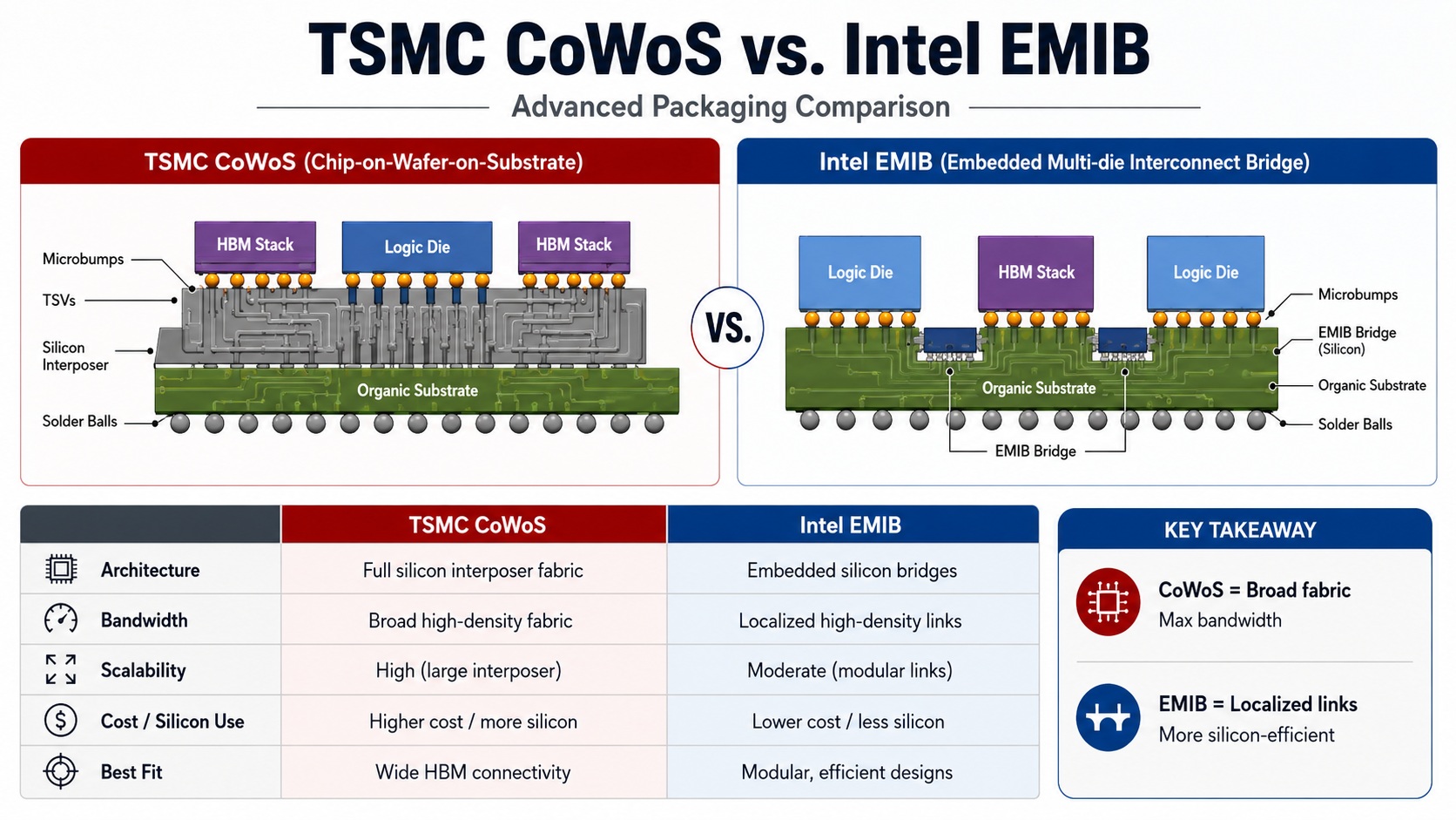
What is the difference between TSMC CoWoS and Intel EMIB?
TSMC CoWoS and Intel EMIB are advanced packaging platforms designed to overcome the economic and physical limits of monolithic system-on-chip scaling. Both enable heterogeneous integration of logic, memory and specialized chiplets within one package, but they use fundamentally different interconnect structures. CoWoS generally creates a broad, high-density interconnect plane beneath the dies, whereas EMIB places small silicon bridges only where adjacent dies require dense communication. This architectural distinction drives differences in bandwidth distribution, package scaling, cost, thermal behavior and design methodology.
CoWoS, meaning Chip-on-Wafer-on-Substrate, is part of TSMC’s 3DFabric portfolio and is widely associated with high-performance computing and artificial-intelligence processors. In CoWoS-S, logic dies and high-bandwidth memory stacks are mounted on a passive silicon interposer containing fine-pitch wiring and through-silicon vias. The interposer is subsequently attached to an organic package substrate. Because almost the entire area under the active dies can provide dense routing, CoWoS-S supports extremely wide parallel interfaces, predictable signal paths and substantial die-to-die connectivity. TSMC states that CoWoS-S supports interposers up to approximately 3.3 reticles, or 2,700 square millimetres, while CoWoS-L and CoWoS-R support larger systems.
The CoWoS family is broader than a single silicon-interposer process. CoWoS-R replaces the large silicon interposer with a multilayer redistribution-layer interposer, reducing dependence on a complete sheet of interposer silicon. CoWoS-L combines an RDL-based interposer with localized silicon interconnect elements in regions requiring greater routing density. These variants allow designers to trade maximum wiring density against package size, cost and manufacturing complexity. Consequently, comparing EMIB only with CoWoS-S understates TSMC’s architectural flexibility. CoWoS-L, in particular, uses localized silicon structures that partially resemble bridge-based packaging. Both CoWoS-R and CoWoS-L entered volume production before or during 2024.
Intel’s Embedded Multi-die Interconnect Bridge embeds small passive silicon bridges inside an organic package substrate. Microbumps connect the edges of neighbouring dies to fine-pitch wiring on each bridge, while conventional substrate traces carry lower-density signals elsewhere. EMIB therefore avoids a package-wide silicon interposer and its associated through-silicon vias. Intel positions EMIB for logic-to-logic and logic-to-HBM integration and reports high-volume production use since 2017. Newer options include EMIB-M, which incorporates metal-insulator-metal capacitance, and EMIB-T, which adds through-silicon vias to the bridge for enhanced vertical connectivity and power delivery.
From an electrical perspective, CoWoS-S offers the most uniform high-density routing environment. A large interposer can distribute thousands of short connections among a central accelerator, multiple HBM stacks and additional chiplets without limiting dense links to die edges facing a bridge. This characteristic is especially valuable when broad connectivity is required across much of the package. The continuous interposer also permits designers to integrate power-distribution structures and decoupling capacitance close to active devices.
EMIB is more silicon-efficient when communication is localized between adjacent dies. It provides short, dense interconnections without paying the silicon-area cost of an interposer beneath components that do not require fine-pitch routing. However, complicated topologies may require multiple bridges, careful chiplet floorplanning and additional organic-substrate traces between nonadjacent components. The package architecture must align bridge locations precisely with the edges and interfaces of each die.
Mechanical and manufacturing trade-offs are similarly nuanced. Eliminating a large silicon interposer can reduce material usage and some wafer-processing operations, giving EMIB potential cost and yield advantages for appropriate designs. Its organic substrate remains difficult to manufacture because bridges must be embedded, planarized and aligned accurately. CoWoS-S adds a large, thin silicon structure whose fabrication, handling, warpage control and known-good-die assembly increase process complexity. Nevertheless, its regular interposer provides a mature and predictable routing platform. CoWoS-R and CoWoS-L attempt to reduce the size, cost and manufacturability constraints of full silicon interposers.
Neither architecture automatically solves heat removal. Both place high-power logic and HBM stacks in close proximity, increasing thermal coupling and local heat density. CoWoS can accommodate large logic-and-memory arrays, but package warpage, power delivery and cooling become harder as the interposer and package expand. EMIB permits relatively flexible die placement and avoids a continuous silicon layer, although thermal performance still depends principally on die power, spacing, heat-spreader design, package materials and system-level cooling.
Both technologies can also support vertical integration. Intel combines EMIB with Foveros die stacking to produce EMIB 3.5D systems containing multiple horizontally and vertically integrated chiplets. TSMC can combine CoWoS with its SoIC wafer-level stacking platform. These combinations allow designers to place cache, logic or specialized functions vertically while using CoWoS or EMIB for package-level horizontal connectivity.
The practical selection criterion is therefore connectivity geometry rather than a simple performance ranking. CoWoS-S is strongest when a system requires a large, continuous and extremely dense interconnect fabric, particularly between accelerators and multiple HBM stacks. CoWoS-R and CoWoS-L extend this approach toward larger or more cost-conscious products. EMIB is strongest when high-bandwidth links are concentrated at particular die boundaries and designers value silicon efficiency, modularity and avoidance of a full interposer.
Bottom line: CoWoS emphasizes an interposer-centric system fabric, while EMIB emphasizes localized silicon bridges embedded in an organic substrate. The better choice depends on interface width, communication topology, package dimensions, power delivery, thermal limits, assembly yield, design-tool support, manufacturing availability and total system cost—not on packaging density alone.
Also Read:
TSMC’s Raises the Bar on CAPEX!
TSMC A16 Backside Power at VLSI 2026
Intel 18A vs Intel 18A-P: What Is the Difference and Why Does It Matter?
Share this post via:



Comments
One Reply to “TSMC CoWoS versus Intel EMIB Semiconductor Packaging”
You must register or log in to view/post comments.