You are currently viewing SemiWiki as a guest which gives you limited access to the site. To view blog comments and experience other SemiWiki features you must be a registered member. Registration is fast, simple, and absolutely free so please,
join our community today!
By Shaurya Seth
Terafab is one of the most ambitious projects of the decade: $16.8 billion for phase one and up to $119 billion across four phases. A research fab in Austin iterates on process recipes, transistor designs, and packaging variants at a few thousand wafers per month. A volume fab in Grimes County targets 100,000 wafer… Read More
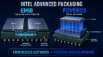
Intel EMIB and Intel Foveros are advanced semiconductor-packaging technologies designed to combine multiple silicon dies, or chiplets, within one processor package. Both support heterogeneous integration: manufacturers can build different functions using the process technology best suited to each one, then connect … Read More
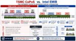
TSMC’s CoPoS, generally described as Chip-on-Panel-on-Substrate, and Intel’s EMIB, or Embedded Multi-die Interconnect Bridge, address the same strategic problem: integrating increasingly large, heterogeneous chiplet systems. However, they attack different physical constraints. CoPoS is an emerging panel-level … Read More
There has been talk at the latest conferences about TSMC customers taking wafers to Intel for packaging. The question is why? Is it competitive pricing? Capacity? Supply chain diversity? CC Wei was asked about this during the last investor call and his perfect response was:
Jeff Su: I guess very simply put, EMIB-T, in his view, is… Read More
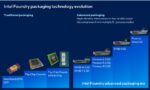
In the rapidly evolving landscape of semiconductor manufacturing, the demand for processors that handle increasing workloads while maintaining power efficiency and compact form factors has never been higher. Intel’s Foveros 2.5D packaging technology emerges as a pivotal innovation, enabling denser die integration… Read More