





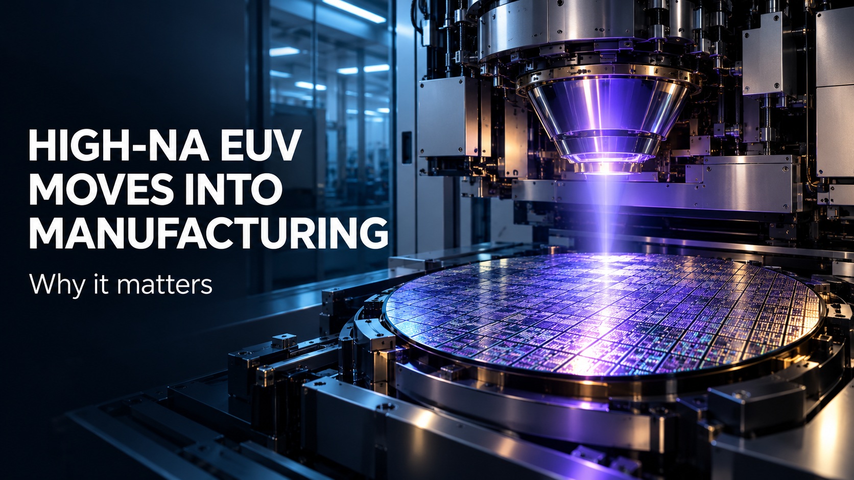
Intel Foundry and ASML say high-numerical-aperture extreme-ultraviolet lithography has crossed an important boundary: it is no longer only a development tool, but a production technology. At the SPIE Photomask Technology and Extreme Ultraviolet Lithography conference, the companies reported that Intel has processed more than one million wafers with High-NA EUV across tool certification, research, development and volume manufacturing. Select layers of Intel Core Ultra Series 3 processors, code-named Panther Lake, are already patterned with the technology.
That milestone matters because lithography determines how densely and accurately a chipmaker can print circuit features on silicon. Conventional EUV production scanners in ASML’s NXE platform use a numerical aperture of 0.33. High-NA systems increase the lens system’s ability to collect and focus diffracted light, improving imaging resolution and giving process engineers more room to print smaller, tighter-pitch structures. Better resolution can reduce reliance on multiple patterning, in which a single complex layer is split across several exposures and process steps. In principle, fewer steps mean shorter cycle times, lower defect risk and simpler process control, although the economic result depends on tool productivity, yield and layer selection.
Intel’s update addresses those practical questions. The company says overlay, throughput and availability are meeting its expectations. Overlay is the accuracy with which one patterned layer aligns to the layers beneath it; small errors can break connections or alter device behavior. Throughput measures how many wafers a scanner can process over time, while availability reflects how consistently the equipment is ready for production. Resolution alone is not enough: a tool must perform on all three dimensions to be commercially useful.
Intel also says High-NA-patterned layers on its Intel 18A process meet or exceed the performance of comparable layers produced on NXE scanners. This does not establish that every layer should move to High-NA. It does suggest that the new platform can be inserted selectively where its imaging advantage justifies the cost and operational complexity, without sacrificing the electrical results expected from the finished chip.
The central technical complication is field size. High-NA optics expose a smaller field than current full-field EUV systems, while the semiconductor supply chain is organized around standard 6-inch photomasks. Intel and ASML describe two near-term approaches. Designers can floor-plan a chip so critical content fits within the available exposure field, or they can use reticle stitching, dividing a larger design across exposures and joining the patterns accurately on the wafer. Intel says its process design kit supports these choices, making the scanner constraint visible to customers during physical design rather than leaving it as a manufacturing-only problem.
For future scaling, the companies support a 6-by-12-inch mask format. A larger mask could carry the content needed for wider High-NA imaging while reducing dependence on stitching, but changing mask dimensions affects far more than the scanner. Mask writers, inspection and repair systems, materials, handling equipment, factory automation, electronic-design-automation software and standards all must evolve together. Intel says it has worked for more than three years with ASML and the wider ecosystem to align that infrastructure.
Why it matters is therefore broader than one processor or one lithography tool. Advanced manufacturing transitions fail when a promising capability cannot be integrated reliably, designed for easily or supplied at scale. Intel’s million-wafer figure provides evidence of operational learning, while production use on Panther Lake offers a concrete product proof point. Support for existing 6-inch masks creates a bridge for customers today; stitching and PDK enablement make that bridge usable; and the proposed larger format establishes a longer-term route to scale.
Bottom line: The announcement does not eliminate High-NA’s economic and engineering risks. For customers, the remaining question is whether those gains translate into yield, cost and schedule predictability across designs. It does show the industry shifting from proving that the optics work to building a repeatable manufacturing system around them. That transition—from resolution demonstration to ecosystem readiness—is what makes the update significant.
SOURCE:
Intel Foundry and ASML Collaborate to Accelerate Industry Readiness for High NA EUV
Also Read:
Comparing Advanced Packaging from TSMC, Intel Foundry, and Samsung Foundry
Intel 18A-P Pushes RibbonFET and Backside Power Beyond the First Generation
Intel’s 14A Is Winning the Race Against Defects
Share this post via:



Comments
3 Replies to “High-NA EUV Moves From Experiment to Manufacturing”
You must register or log in to view/post comments.