You are currently viewing SemiWiki as a guest which gives you limited access to the site. To view blog comments and experience other SemiWiki features you must be a registered member. Registration is fast, simple, and absolutely free so please,
join our community today!
The semiconductor industry has experienced rapid advancements in recent years, particularly with the increasing demand for high-performance computing, artificial intelligence, and advanced automotive systems. Traditional single-die chip designs are often unable to meet modern PPA requirements. As a result, engineers… Read More
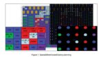
Introduction of 2.5D and 3D multi-die based products are helping extend the boundaries of Moore’s Law, overcoming limitations in speed and capacity for high-end computational tasks. In spite of its critical function within the 3DIC paradigm, the interposer die’s role and related challenges are often neither fully comprehended… Read More
In the 3D-IC (Three-dimensional integrated circuit) chip design method, chiplets or wafers are stacked vertically on top of each other and are connected using Through Silicon Vias (TSVs) or hybrid bonding.
The 2.5D-IC design method places multiple chiplets alongside each other on a silicon interposer. Microbumps and interconnect… Read More
The pace of Moore’s Law scaling for monolithic integrated circuit density has abated, due to a combination of fundamental technical challenges and financial considerations. Yet, from an architectural perspective, the diversity in end product requirements continues to grow. New heterogeneous processing units are being… Read More