






Why Optical Probing Is Becoming a Manufacturing Boundary for Silicon Photonics
Silicon photonics has already shown that extremely precise optical alignment is possible.
In controlled laboratory environments, engineers can align fibers, waveguides, grating couplers, edge couplers, modulators, detectors, and electrical probes with remarkable accuracy. They can measure insertion loss, coupling efficiency, optical power, bandwidth, modulation response, detector sensitivity, and high-speed electrical behavior.
That level of precision is impressive.
But precision alone does not create scale.
The harder question is whether the same optical result can be reproduced across many devices, wafers, operators, tools, calibration cycles, and production lots.
A successful measurement once demonstrates capability.
A repeatable measurement thousands of times creates evidence.
That distinction is becoming increasingly important as silicon photonics moves from research demonstrations toward co-packaged optics, optical I/O, photonic integrated circuits, and high-volume AI infrastructure.
Why Photonics Probing Is Different
Electrical wafer probing is already a demanding precision activity. Probe tips must contact small pads without damaging the device, introducing excessive resistance, or creating unstable measurements.
Photonics adds another layer of sensitivity.
The test system may need to align an optical fiber or fiber array to a coupler whose performance changes with very small variations in position, height, angle, polarization, wavelength, or temperature.
A shift that appears insignificant mechanically can materially change the optical measurement.
The challenge becomes even greater when optical and electrical behavior must be measured together.
A modulator, for example, may require:
- optical input and output coupling
- high-speed electrical drive signals
- DC bias control
- RF probing
- polarization management
- thermal stabilization
- optical-power measurement
- bandwidth or modulation-response analysis
The result depends not only on the device.
It also depends on the alignment method, probe condition, fiber position, calibration state, optical path, test sequence, environmental stability, and software controlling the measurement.
This makes the probe platform part of the evidence chain.
What a Photonics Probe Platform Actually Does
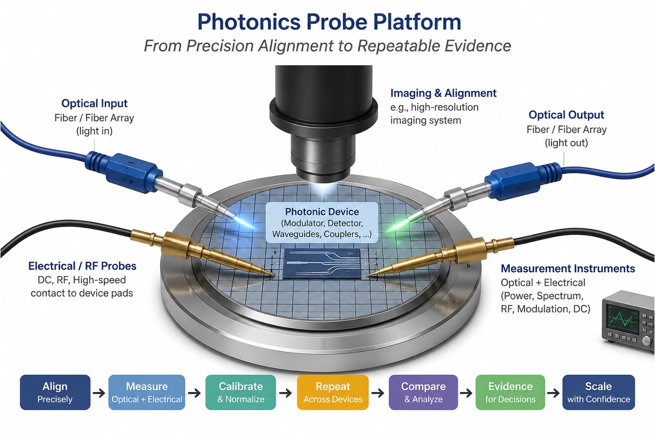
A modern photonics probe station brings several capabilities together around the device under test.
The wafer or die is positioned on a controlled stage. Electrical probes contact the relevant pads. Optical fibers, fiber arrays, or specialized optical probes couple light into and out of the photonic structure. Imaging systems help locate alignment features. Motion systems search for the best coupling position. Calibration routines establish reference conditions. Measurement instruments collect the optical and electrical response.
The system may support:
- vertical coupling through grating couplers
- edge coupling into waveguides
- wafer-level and die-level testing
- DC, RF, and optical co-test
- modulator and detector characterization
- automated alignment and realignment
- calibration and reference measurements
- repeated measurements across a wafer map
The purpose is not simply to find the highest optical power once.
The purpose is to turn alignment and measurement into a controlled process.
That means defining how the system approaches the device, how it searches for coupling, how it determines the measurement position, how it compensates for drift, how it verifies calibration, and how it records the result.
Platforms from companies such as FormFactor illustrate this transition from expert-driven optical alignment toward automated and repeatable photonics probing.
The equipment matters, but the deeper change is methodological.
Photonics testing is moving from an individual expert obtaining a good result to a measurement system producing comparable evidence.
Accuracy and Repeatability Are Not the Same
A measurement can be accurate once and still be unsuitable for manufacturing.
Suppose a probe station measures excellent coupling efficiency on one device. That result may be correct. But if the same device produces materially different readings when measured again, confidence in the process remains limited.
Manufacturing requires answers to additional questions:
Can the same device be measured repeatedly with similar results?
Can another tool reproduce the measurement?
Can another operator run the same process?
Can measurements from different wafers and lots be compared?
Can the system distinguish device variation from measurement-system variation?
This last question is critical.
When measured insertion loss changes, did the device change?
Did the fiber move?
Did polarization drift?
Did the optical source change?
Did the calibration reference age?
Did temperature move the operating point?
Did the probe contact alter the electrical response?
Without measurement repeatability, the industry cannot confidently separate product variation from test variation.
That makes repeatability more than an equipment specification. It becomes a condition for manufacturing decisions.
From Alignment to Evidence
The traditional photonics test objective is often expressed as:
Align the light and measure the device.
The manufacturing objective is broader:
Align, measure, calibrate, repeat, compare, and preserve the conditions behind the result.
That requires the test system to capture more than a final number.
Useful manufacturing evidence may include:
- alignment position and search history
- optical input power
- polarization state
- wavelength and spectral conditions
- stage and chuck temperature
- electrical bias and drive settings
- calibration status
- probe and fiber identification
- measurement uncertainty
- device location and wafer context
- repeated-measurement variation
A coupling-loss value without its measurement conditions may be difficult to compare with another result.
A calibrated and repeatable value connected to its operating conditions can support yield analysis, process improvement, qualification, and product release.
This is the transition from measurement data to manufacturing evidence.
Why Automation Matters
Manual photonics alignment can produce excellent results, especially in development laboratories where skilled engineers can interpret visual and measurement feedback.
But manual expertise is difficult to scale.
High-volume manufacturing cannot depend on one person recognizing the correct fiber angle, deciding when coupling is good enough, or manually compensating for drift.
Automation converts tacit expertise into a repeatable sequence.
An automated platform can:
- locate the device
- approach the coupling region safely
- search for optical power
- optimize position and angle
- verify electrical contact
- apply calibration
- execute the measurement sequence
- detect an abnormal result
- realign or recalibrate when required
- store the evidence with the device record
This does not eliminate engineering judgment.
It moves engineering judgment into the design of the measurement process.
The quality of the automation then becomes part of product quality.
The Hidden Boundary in CPO and Optical I/O
For co-packaged optics and optical I/O, the photonic device is only one part of a larger realization problem.
The modulator may perform well.
The detector may respond correctly.
The optical coupling structure may meet its simulated target.
The electrical interface may pass its individual test.
But the product is not ready merely because each element works once.
The manufacturer must know whether those results can be reproduced after assembly, across temperature, after calibration, through process variation, and over the expected operating life.
Photonics probing therefore sits at an important boundary between:
- device design and manufacturing
- optical performance and package integration
- laboratory alignment and production automation
- individual measurements and release decisions
- component capability and system confidence
This boundary is easy to underestimate because probing is often viewed as a downstream test activity.
In reality, the probing strategy can influence device layout, coupler placement, pad access, fiber-array geometry, calibration structures, test time, packaging sequence, and known-good-die strategy.
Testability must therefore enter the design flow early.
A photonic architecture that is difficult to probe, calibrate, or compare may also be difficult to manufacture economically.
Repeatability Enables Learning
Repeatable probing does more than screen devices.
It allows the manufacturing system to learn.
When measurements are performed under controlled conditions, engineers can identify patterns across wafers and lots.
They can determine whether variation originates from lithography, etch, deposition, bonding, optical coupling, metallization, packaging, or test setup.
They can track whether a process adjustment improves performance or merely changes the measurement condition.
They can compare device behavior before and after assembly.
They can connect wafer-level results with package-level and system-level performance.
Without repeatability, each measurement risks becoming an isolated observation.
With repeatability, measurements become comparable evidence.
Comparable evidence enables process learning.
Process learning enables yield improvement.
From Precision to Scale
The silicon photonics industry does not need to prove only that light can be aligned.
That has already been demonstrated.
The next challenge is proving that light can be aligned, measured, calibrated, and trusted repeatedly across production.
This is why photonics probe platforms matter.
They are not merely microscopes, stages, fibers, and instruments assembled around a wafer.
They are part of the infrastructure required to transform optical performance into manufacturing confidence.
The progression is straightforward:
Precision creates the first result
Repeatability creates confidence
Confidence creates manufacturing evidence
Manufacturing evidence enables scale
For CPO, optical I/O, silicon photonics, and photonic integrated circuits, this may become one of the most important hidden realization boundaries.
The future of photonics manufacturing will not be determined only by how precisely a device can be aligned in the laboratory.
It will be determined by whether that precision can be converted into a repeatable, automatable, and trusted evidence path.
That is when photonics probing becomes more than test.
It becomes part of product realization.
Also Read:
The Packaging PDK Is the Missing Layer for Co-Packaged Optics
The Modulator Is Not the Product: Why AI Photonics Needs an Electro-Optical Realization Corridor
A tower-like heterogeneous packaging architecture for the AI era
Share this post via:



Rethinking Phase Jitter: An Algorithmic Approach to Signal Integrity