







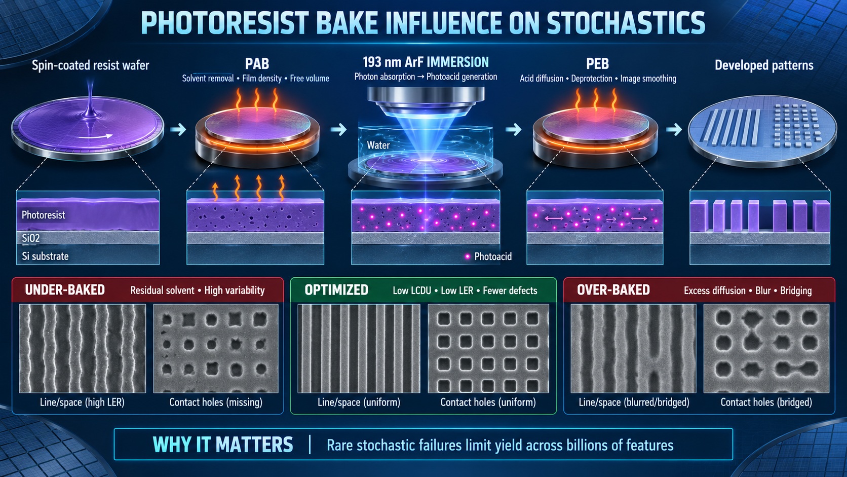
Deep-ultraviolet (DUV) immersion lithography remains a critical patterning technology for advanced semiconductor manufacturing. Using a 193 nm ArF exposure system with water between the projection lens and wafer, immersion lithography increases numerical aperture and enables smaller features than dry exposure. However, as feature dimensions shrink, random—or stochastic—variations increasingly determine pattern quality and yield. Although photon shot noise is a fundamental contributor, resist-processing conditions, particularly bake steps, strongly influence how microscopic fluctuations become printable defects.
A chemically amplified photoresist normally experiences two important thermal processes: the post-apply bake (PAB) and post-exposure bake (PEB). PAB removes casting solvent, stabilizes the resist film, and establishes its initial density and free volume. PEB activates acid-catalyzed deprotection reactions after exposure and permits the photo-generated acid to diffuse through the polymer matrix. Consequently, bake temperature, duration, heating rate, cooling rate, and wafer-temperature uniformity can all affect critical dimension (CD), line-edge roughness (LER), local CD uniformity (LCDU), and stochastic-defect probability.
The PAB condition determines the physical and chemical state of the resist before exposure. Insufficient baking can leave excess solvent, producing nonuniform density, altered dissolution behavior, and greater molecular mobility. Residual solvent may also change acid generation efficiency or promote acid diffusion during PEB. Conversely, an excessively hot or prolonged PAB can reduce free volume, modify resist-component distributions, or cause premature loss of volatile species. These changes may influence sensitivity and image contrast even when the mean printed CD appears acceptable. Thus, identical average CDs can conceal different stochastic signatures.
PEB has an especially direct relationship with stochastic behavior. During exposure, absorbed photons generate acid molecules at discrete locations. Their initial number and spatial distribution fluctuate statistically. During PEB, acid diffusion smooths this discrete chemical image, while catalytic deprotection amplifies it. Greater diffusion can average local fluctuations and reduce high-frequency roughness, but excessive diffusion blurs feature boundaries, increases tip-to-tip variation, and can cause bridging or contact-hole closure. Restricted diffusion preserves resolution but may leave isolated regions insufficiently reacted, increasing missing-hole defects or broken lines. The bake therefore establishes a trade-off between chemical-image smoothing and loss of image fidelity.
A systematic study should independently vary PAB and PEB temperatures and times while holding resist thickness, exposure dose, focus, developer conditions, substrate stack, and scanner settings constant. A designed experiment can also examine temperature ramp and delay between exposure and PEB. Dense lines, isolated lines, contact holes, and line-space patterns should be included because each geometry responds differently to diffusion and dissolution variability.
Characterization must extend beyond wafer-level mean CD. Critical outputs include LCDU distributions, LER and line-width roughness, defect counts, contact-hole failure probability, exposure latitude, and process-window area. High-volume scanning electron microscopy can provide statistically meaningful populations, while defect probability should be evaluated across many thousands or millions of features. Fitting distribution tails is particularly important because manufacturing yield is governed by rare failures rather than average behavior. Resist-thickness measurements, residual-solvent analysis, and thermal-wafer mapping can help connect observed variability to physical mechanisms.
The expected result is not simply one bake temperature that minimizes every metric. Instead, the study should identify a robust operating region in which stochastic failures are suppressed without unacceptable loss of resolution, sensitivity, or process latitude. Interaction effects are likely: a PAB condition that changes solvent content or resist density can alter the diffusion response during PEB. Optimizing the two bakes independently may therefore miss the best combined condition.
Bottom line: This work matters because stochastic defects are becoming a practical scaling limit for optical lithography. A process may satisfy conventional CD targets yet still fail economically because rare missing contacts, bridges, or line breaks occur across billions of patterned features. Bake optimization is comparatively inexpensive and can improve performance without changing the scanner, mask, or resist platform. Understanding thermal effects also improves process transfer between tracks and fabs, where small differences in hotplate calibration or wafer handling can produce large changes in defect tails. By linking bake history to stochastic mechanisms, manufacturers can establish tighter controls, more predictive models, and higher-yielding DUV immersion processes.
Also Read:
Five Billion Pulses Later: What DUV Optics Testing Reveals About Semiconductor Tool Uptime
Huawei Can’t Shrink Its Chips, So It’s Folding Them
Reducing EUV Exposure Dose Through Underlayer Engineering
Share this post via:



ChipAgent Raises $134Million and Why it Matters