




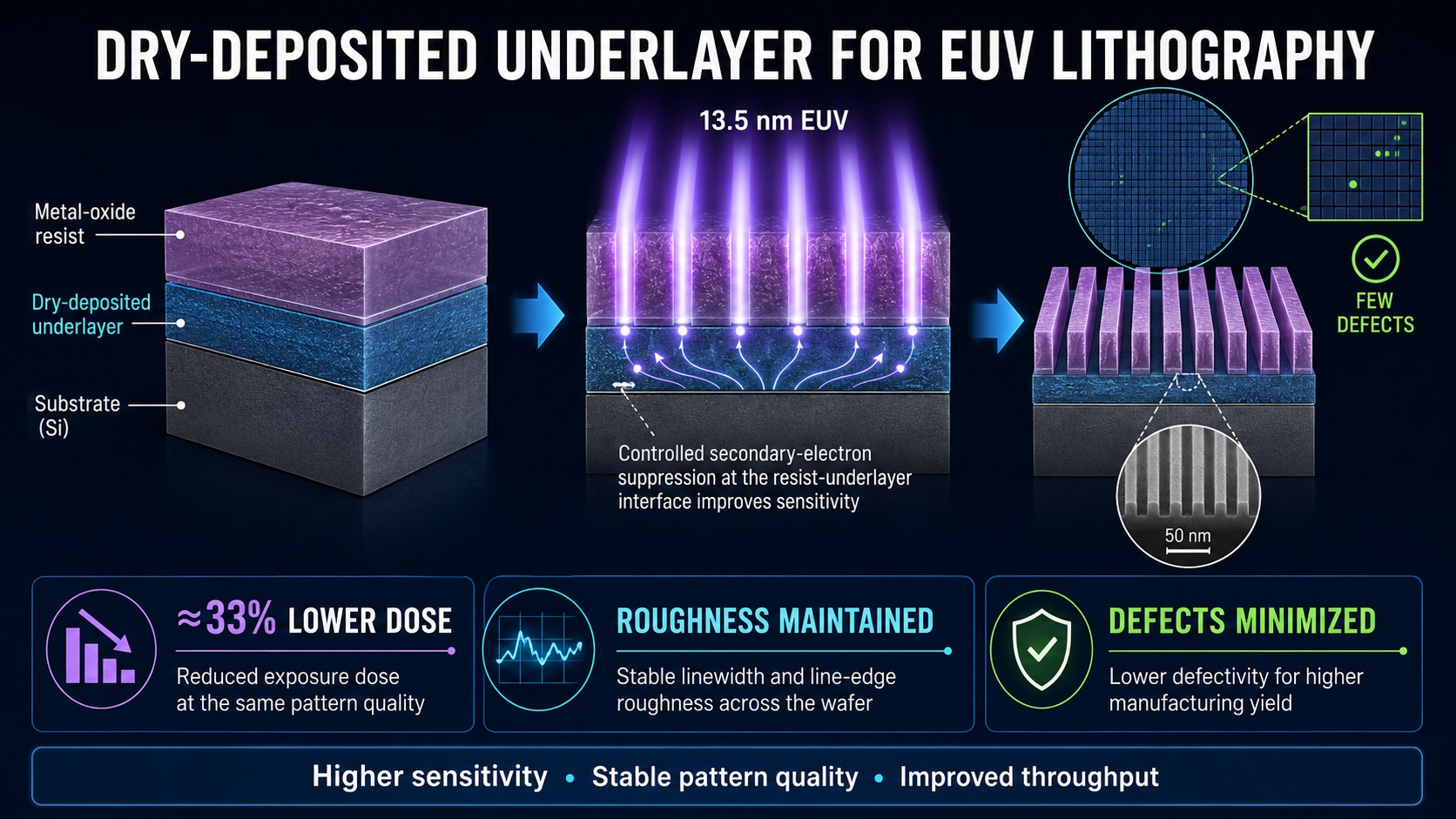



Extreme-ultraviolet lithography is essential for manufacturing advanced semiconductor devices, but its continued scaling presents a difficult materials problem. Photoresists must simultaneously provide high resolution, low exposure dose, limited line-edge or linewidth roughness, and extremely low defectivity. These requirements often conflict: lowering the EUV dose improves scanner throughput but increases stochastic variation because fewer photons participate in forming each feature. The SPIE paper “Substantial dose reduction using dry deposited underlayer for EUV lithography while maintaining roughness and minimizing defects,” by Achintya Kundu and colleagues, examines whether engineering the layer beneath the photoresist can improve this balance.
An underlayer is a thin film positioned between the wafer substrate and the EUV resist. Although it does not directly define the printed pattern, its physical and chemical properties influence resist adhesion, electron generation, energy transfer, development behavior, and pattern stability. Conventional underlayers are normally deposited by wet, spin-coating processes. A dry-deposited film, however, can offer better control of thickness and composition while avoiding solvents and some of the variability associated with liquid coating. It may also be easier to integrate into increasingly thin resist stacks required for high-numerical-aperture EUV lithography.
The researchers investigated a dry-deposited organic underlayer used with a metal-oxide resist. Metal-oxide resists are attractive because their inorganic constituents absorb EUV radiation efficiently and provide strong resistance during plasma etching. Nevertheless, they can require relatively high exposure doses and remain vulnerable to stochastic defects, roughness, and pattern collapse. The purpose of the dry underlayer was therefore not simply to support the resist mechanically. It was designed to modify the resist–substrate interface and make more effective use of the energy delivered during exposure.
The study’s most important result was a substantial reduction in the dose needed to print the target dimensions. Related reporting of this underlayer platform describes an approximately 33 percent reduction in required EUV dose when it is combined with a metal-oxide resist. Such an improvement is industrially significant because EUV exposure dose is closely connected to scanner throughput. If the resist reaches the required critical dimension with less incident energy, more wafers can potentially be exposed within a given period, improving manufacturing productivity and lowering the cost per patterned layer.
Dose reduction alone, however, would not constitute a useful advance if it produced unacceptable roughness. At low photon counts, statistical fluctuations can cause variations in the resist reaction and create irregular feature boundaries. The authors therefore evaluated roughness alongside sensitivity. Their results indicate that the dry-deposited underlayer preserved roughness performance even as the dose-to-size decreased. This suggests that the sensitivity improvement was not obtained simply by lowering the imaging threshold until noisy, poorly defined patterns appeared. Instead, the underlayer improved the overall response of the material stack while retaining pattern quality.
Defectivity was another central consideration. EUV patterns may contain missing or merged features, bridges between lines, breaks, microbridges, or local failures caused by stochastic variations and resist-processing interactions. Because a modern integrated circuit contains enormous numbers of features, even an apparently small defect probability may be unacceptable. The study therefore considered defects across the usable exposure range rather than relying only on average critical-dimension measurements. The dry underlayer minimized observed defects and helped maintain a practical process window, demonstrating that increased sensitivity did not necessarily demand a defectivity penalty.
Several mechanisms may contribute to this behavior. The underlayer can alter the production and transport of secondary electrons generated when EUV photons interact with the material stack. These electrons participate in the chemical transformations that determine resist solubility. The film can also influence interfacial energy, adhesion, and development kinetics. A chemically and physically uniform dry-deposited surface may consequently promote more consistent reactions at the bottom of the resist, reduce local variability, and support faithful pattern formation in thin films.
Overall, the paper shows that EUV performance should be optimized at the stack level rather than by treating the photoresist as an isolated material. A properly engineered dry-deposited underlayer can reduce exposure demand while maintaining roughness and suppressing defects—the three outcomes needed for commercially meaningful progress. The approach is especially relevant to high-NA EUV, where thinner films, smaller features, reduced depth of focus, and tighter defect limits will make interface control increasingly important. The work therefore identifies underlayer engineering as a promising route toward faster, more economical, and more reliable fabrication at future semiconductor nodes.
Full Paper can be accessed here.
Also Read:
ASML’s Path to Lithography Dominance—and the Coming Maskless Revolution
Intel and TSMC Take Different Paths to High-NA EUV
Crossing the Yield Cliff: IDP V6 and the Future of Manufacturing Forecasting
Share this post via:



SEMICON West’s Autonomous Fab Vision Needs a Decision-Escalation Design