







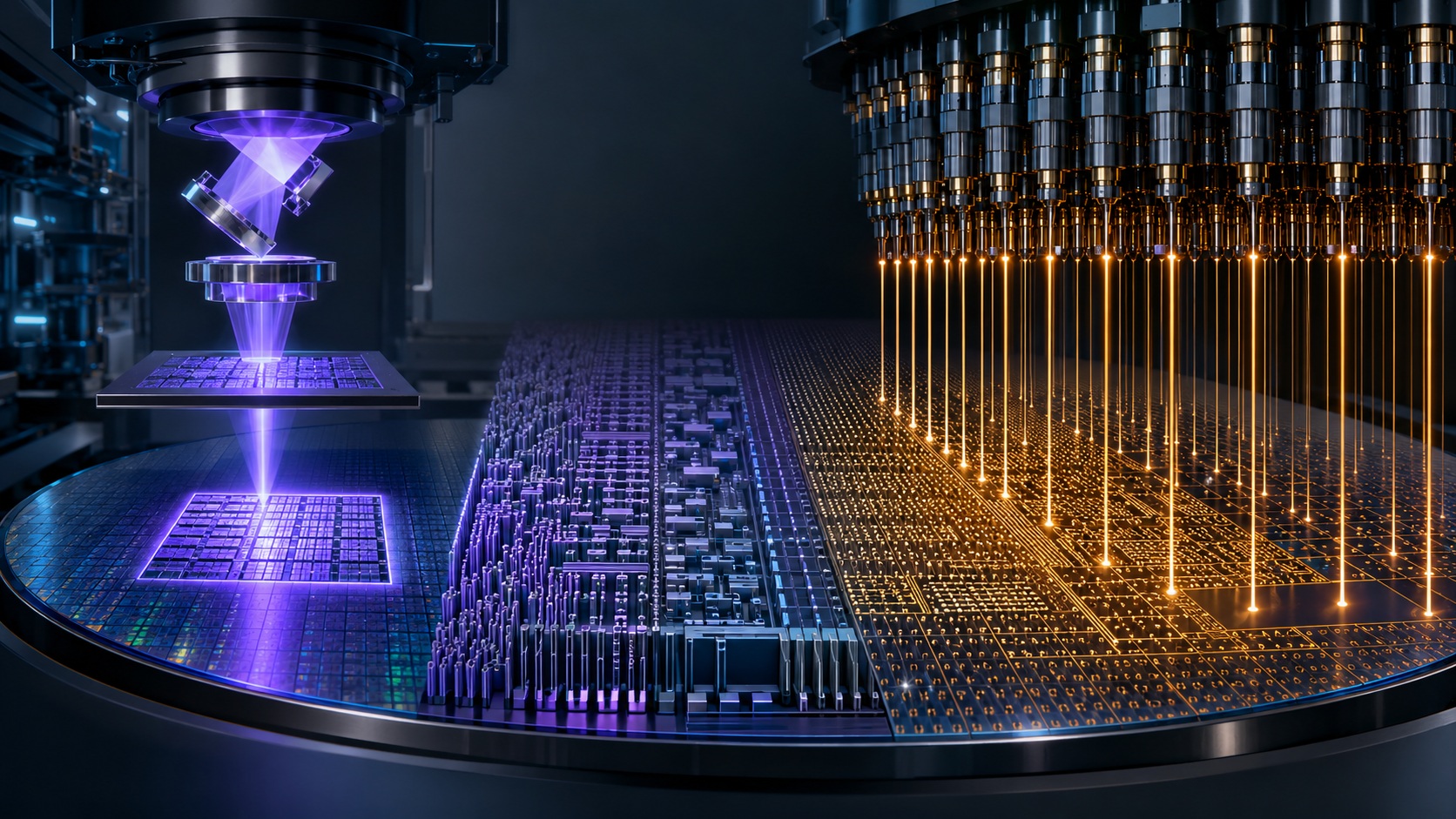
ASML’s dominance was not born from a single invention. It emerged from four decades of systems engineering, supplier orchestration, and repeated bets on lithographic transitions that competitors judged too expensive. Founded in 1984 as a Philips–ASM joint venture, the Dutch company first differentiated itself with modular wafer steppers, then exploited the shift from step-and-repeat tools to faster step-and-scan systems. By the late 1990s, its TWINSCAN architecture aligned two wafer stages: one wafer could be measured while another was exposed, raising throughput without sacrificing overlay.
The decisive advance was immersion lithography. Conventional deep-ultraviolet scanners use 193-nanometer argon-fluoride light; placing ultrapure water between the final lens and wafer increases numerical aperture and therefore resolution. ASML commercialized immersion aggressively, while computational lithography, optical proximity correction, and multiple patterning extended 193-nanometer tools far beyond their apparent physical limit. Its 2013 acquisition of Cymer secured the laser source, and its close integration with Zeiss optics created a supplier network whose tolerances, interfaces, and accumulated process knowledge became extremely difficult to reproduce.
Extreme ultraviolet lithography deepened that moat. EUV uses 13.5-nanometer radiation generated by firing high-power laser pulses at microscopic tin droplets. Because EUV is absorbed by air and glass, the exposure path operates in vacuum and uses multilayer reflective mirrors rather than refractive lenses. Each mirror sacrifices photons; contamination, stochastic resist effects, mask defects, source power, overlay, and uptime all had to be solved simultaneously. ASML coordinated thousands of specialists and billions of euros of customer and supplier investment until EUV became viable for high-volume manufacturing.
The resulting platform is more than a scanner. It is an integrated control system combining light generation, nanometer-precision mechatronics, thermal management, vacuum engineering, metrology, and software that corrects distortions across mask, lens, wafer, and process. High-NA EUV raises numerical aperture from 0.33 to 0.55, targeting roughly 8-nanometer resolution and reducing some costly multi-patterning steps. This reinforces ASML’s position: customers are buying not simply wavelength, but yield, throughput, service data, and a roadmap synchronized with leading fabs.
Yet the next disruption may be maskless. Today’s projection lithography transfers a reticle pattern across many dies, making it extraordinarily productive once the mask exists. The weakness is mask economics. Advanced EUV masks require complex correction, inspection, repair, pellicles, and long qualification cycles. For low-volume chips, rapid design revisions, heterogeneous integration, advanced packaging, photonics, and research, that fixed cost and delay can dominate.
Maskless lithography sends digital pattern data directly to the substrate using electron beams, ion beams, scanned lasers, or programmable micromirror arrays. Its central trade-off is throughput: serial writing offers exquisite resolution but is far slower than exposing an entire field. The plausible revolution therefore depends on massive parallelism. Multi-beam electron systems divide the data stream among hundreds of thousands—or eventually millions—of independently controlled beamlets, while high-speed computation performs real-time proximity correction, dose modulation, stitching, and defect compensation.
The first impact is likely evolutionary, not an immediate replacement for EUV. Multi-beam tools already accelerate production of the masks that EUV scanners consume. Direct write is better positioned initially for mask repair, prototyping, custom layers, chiplets, interposers, and low-volume accelerators, where eliminating a reticle can outweigh slower wafer throughput. Digital exposure also enables per-die personalization and rapid correction of substrate distortion, capabilities a fixed mask cannot easily provide.
That transition will be governed less by headline resolution than by cost per correctly patterned layer, including cycle time, yield learning, energy, and flexibility across product volumes and architectures in practice.
Bottom line: For leading-edge, high-volume logic, ASML’s optical replication advantage remains formidable. A maskless challenger must match nanometer resolution, overlay, defectivity, resist sensitivity, and hundreds of wafers per hour while moving and processing immense data volumes. The coming revolution is therefore unlikely to abolish ASML. More probably, lithography becomes hybrid: EUV prints dense, repeated layers; maskless tools write variable or economically awkward ones. ASML achieved dominance by industrializing impossible physics. Its next challenge is recognizing when computation and parallel direct writing make the mask optional.
Also Read:
Intel and TSMC Take Different Paths to High-NA EUV
ASML High-NA EUV is Not Ready for High-Volume Production
Beyond Moore’s Law: High NA EUV Lithography Redefines Advanced Chip Manufacturing
Share this post via:




The silent killer of analog reliability: Why SPICE misses floating net