





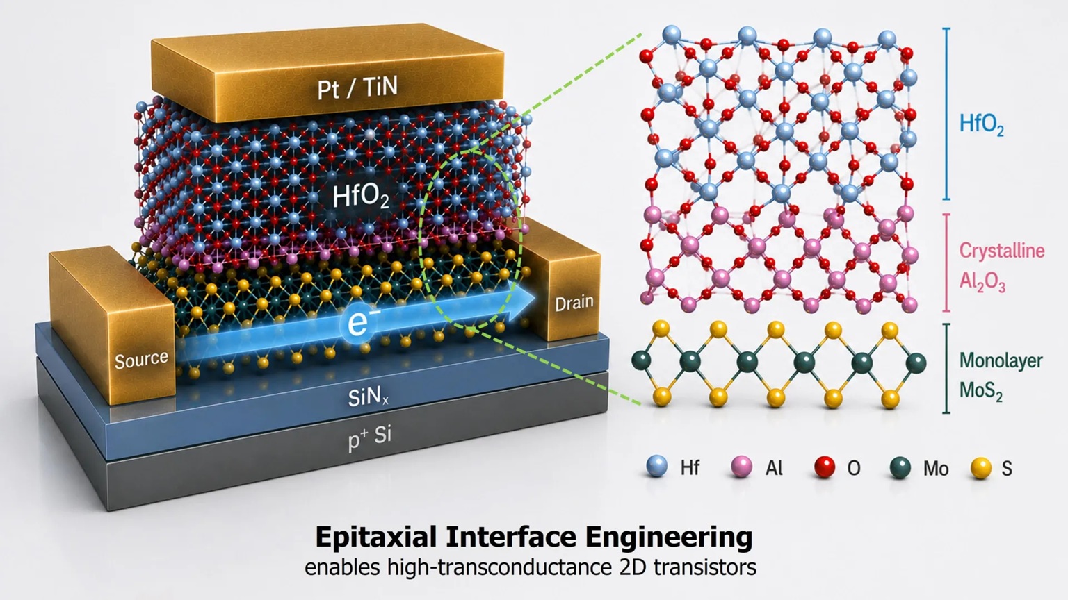
Researchers at National Yang Ming Chiao Tung University and TSMC Corporate Research engineered a 0.42-nanometer aluminum-oxide interface that protects electron transport in monolayer MoS₂ transistors while enabling strong gate control.
Silicon transistors are approaching physical limits that make each new generation harder to scale. Two-dimensional semiconductors such as monolayer molybdenum disulfide (MoS₂) offer a possible route forward because their channels can be only one atomic layer thick without losing useful electronic behavior. Their practical performance, however, has been constrained by a less visible component: the interface between the semiconductor channel and the gate dielectric.
A field-effect transistor uses a gate electrode to modulate current through a channel. Between the gate and channel lies an insulating dielectric. Reducing the dielectric’s equivalent oxide thickness, or EOT, strengthens the gate’s electrostatic control, helping suppress short-channel effects and lowering operating voltage. In conventional silicon technology, mature oxidation and deposition processes produce high-quality interfaces. Monolayer MoS₂ presents a different challenge. Its van der Waals surface lacks dangling bonds, so deposited dielectric materials do not readily nucleate into a uniform film.
Poor nucleation can create gaps, defects, charge traps, and local electrical disorder. These imperfections increase leakage and hysteresis and scatter carriers moving through the MoS₂. Engineers therefore face a difficult tradeoff: a thinner dielectric improves gate control, but aggressive dielectric deposition can degrade carrier mobility and erase the channel’s intrinsic advantages.
Researchers at National Yang Ming Chiao Tung University and TSMC Corporate Research addressed this problem by treating the interface as an engineered device layer rather than a passive boundary. They deposited an ultrathin epitaxial aluminum layer directly on chemical-vapor-deposition-grown monolayer MoS₂, then oxidized it to form approximately 0.42 nanometers of aluminum oxide. A high-κ hafnium oxide dielectric was subsequently deposited above this interfacial layer.
The oxidized aluminum performs two functions. First, it supplies a smooth, continuous surface on which hafnium oxide can grow uniformly. Second, it acts as an atomic-scale buffer, limiting detrimental interactions between the high-κ dielectric and the semiconductor. The approach preserves electron transport while enabling a dielectric stack thin enough for strong electrostatic coupling.
Using this structure, the team fabricated short-channel, top-gate MoS₂ transistors with an EOT of about one nanometer. Devices with channel lengths near 100 nanometers achieved maximum transconductance of 0.45 millisiemens per micrometer, together with low gate leakage and minimal hysteresis. Transconductance measures how effectively gate voltage changes channel current; a high value therefore indicates strong gate authority and useful drive performance.
The result is important not because 0.42 nanometers defines the transistor’s gate length, but because it is the thickness of the engineered aluminum-oxide interface. That distinction matters: the advance does not represent a complete 0.42-nanometer transistor. Instead, it removes a major obstacle to scaling the dielectric system used with atomically thin channels.
Manufacturability also strengthens the work’s relevance. Many high-performance demonstrations rely on small MoS₂ flakes mechanically exfoliated from bulk crystals. Here, the researchers used CVD-grown monolayer material, a method more compatible with large-area and potentially wafer-scale processing. Significant challenges remain, including uniformity, defect control, contact resistance, reliability, process integration, and reproducibility across full wafers.
Even so, the study reframes a central problem in post-silicon electronics. At atomic dimensions, device behavior depends not only on the properties of individual materials but also on how their electron states, defects, and bonding environments interact across boundaries. An interface only a few atoms thick can determine whether a promising semiconductor delivers laboratory mobility or useful transistor performance.
Further optimization could target subthreshold swing, threshold-voltage stability, and source-drain contacts, all critical to energy-efficient switching. The interface must also survive thermal processing and prolonged electrical stress. Meeting those requirements would determine whether the laboratory structure can become a repeatable manufacturing module for chips.
The broader lesson is that future scaling may depend as much on interface architecture as on discovering new channel materials. By combining monolayer MoS₂, a 0.42-nanometer interfacial oxide, and a high-κ gate dielectric, the researchers demonstrated unusually strong electrostatic control without sacrificing transport. That balance moves two-dimensional transistors closer to practical low-power logic beyond silicon.
You can read the full paper here.
Also Read:
Intel and TSMC Take Different Paths to High-NA EUV
The Difference Between TSMC CoWoS-S and CoWoS-R
TSMC CoPoS Versus Intel EMIB Semiconductor Packaging
The Silicon Shield Has Never Been Stronger!
Share this post via:



Comments
There are no comments yet.
You must register or log in to view/post comments.