





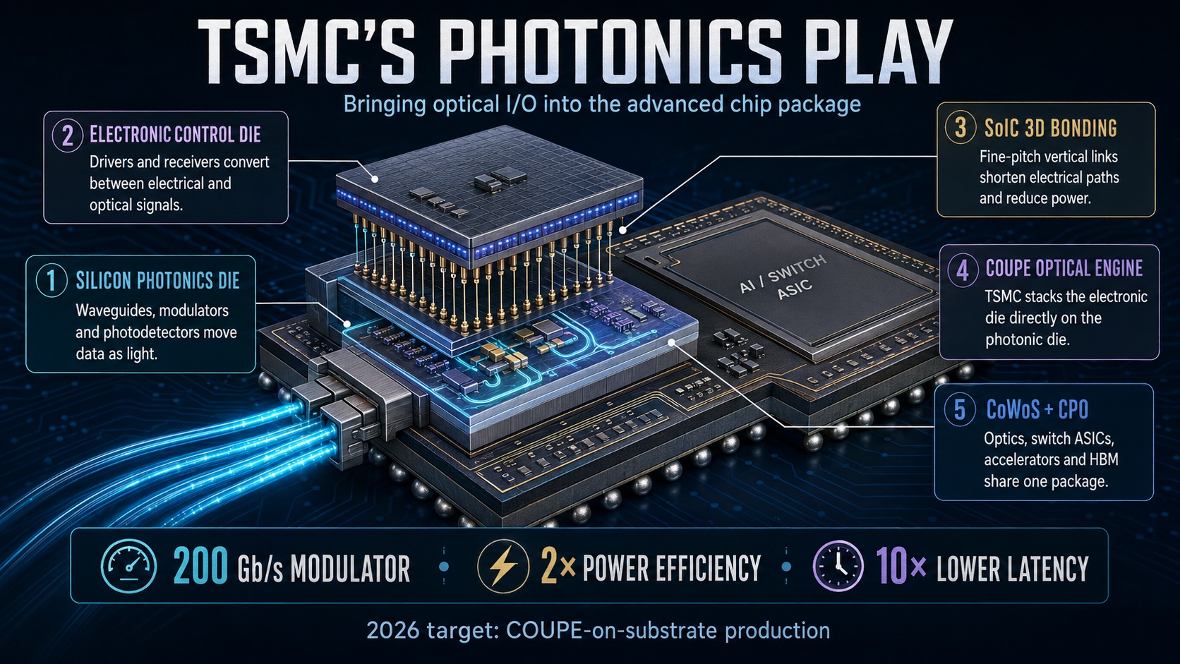
TSMC’s photonics strategy is centered on integrating optical input-output with advanced logic, rather than selling conventional optical transceivers as standalone products. The company is developing a silicon-photonics foundry platform and a packaging architecture called TSMC-COUPE, or Compact Universal Photonic Engine, aimed primarily at AI and high-performance-computing interconnects.
A silicon-photonics die implements optical waveguides, modulators, photodetectors and fiber-coupling structures using semiconductor manufacturing techniques. However, it still requires electronic circuitry for modulation drivers, receiver amplification, clocking and control. In many optical modules, the electronic integrated circuit and photonic integrated circuit are separate dies connected laterally or through package wiring. Those connections add parasitic resistance, capacitance and inductance, increasing power and limiting signaling speed.
COUPE addresses that interface by vertically stacking an electronic die on a photonic die with TSMC’s SoIC chip-on-wafer bonding technology. Fine-pitch, high-density connections shorten the electrical path between driver or receiver circuits and optical devices. TSMC says the structure supports both grating and edge fiber couplers while avoiding cavities and mechanically weak features. The optical engine can then be integrated beside a host ASIC in a larger package.
TSMC has pursued a staged commercialization plan. The first implementation targeted small-form-factor pluggable optics, providing a lower-risk environment for process qualification, device characterization, assembly and reliability testing. The next step is true co-packaged optics, or CPO, in which the optical engines move from the circuit board into the switch or compute package. TSMC announced that a COUPE-on-substrate CPO solution is entering production in 2026.
The company reports that in-package COUPE provides twice the power efficiency and one-tenth the latency of a pluggable board-level implementation. Its platform includes a 200-gigabit-per-second micro-ring modulator, a compact resonant device that converts an electrical data stream into optical modulation. TSMC’s 2025 reporting also says it achieved 200-gigabit-per-second operation with multiple customers and is developing CPO to reduce data-center data-movement energy by more than 50 percent.
Photonics is being tied directly to TSMC’s 3DFabric portfolio. SoIC supplies vertical die-to-die integration; CoWoS can combine optical engines, switch or accelerator ASICs, chiplets and high-bandwidth memory on an interposer and substrate. This is strategically important because an optical link cannot be optimized independently of SerDes circuits, package routing, power delivery, cooling, fiber attachment and test. TSMC can co-design those interfaces while using manufacturing infrastructure already developed for large AI packages.
The immediate application is scale-out networking between racks and potentially scale-up connectivity among accelerators. Electrical channels become progressively harder to drive as data rates and distances increase: insertion loss rises, equalization grows more complex, and retimers consume additional power. Moving the electro-optical conversion closer to the ASIC reduces the length of high-speed copper channels. Optical fiber then carries bandwidth over distance with lower loss.
Significant challenges remain. Micro-ring modulators are compact and efficient but sensitive to fabrication variation and temperature, requiring wavelength control. External lasers must deliver stable optical power without creating thermal or reliability problems inside the package. Fiber attach demands micrometer-scale alignment, while known-good-die screening, optical testing, repairability and yield become difficult when expensive logic and photonics are combined. CPO also changes field service: a failed optical engine cannot be replaced as easily as a pluggable transceiver.
TSMC is separately researching more ambitious photonic computing. It has reported a wafer-integrated digital optical computing system using multilayer photonic fan-out and stacked electronic-photonic dies, with less than 0.08 picojoules per multiply-accumulate operation in an eight-bit, 512-by-512 demonstration. That work is exploratory, whereas COUPE is the near-term commercial focus.
Bottom line: TSMC is treating photonics as a system-integration problem. Its competitive asset is not any single modulator or waveguide. It is the ability to combine a qualified photonics process, electronic control silicon, three-dimensional bonding, interposers, advanced packaging and high-volume manufacturing into a customer-ready platform. That positioning lets fabless chip companies adopt optical connectivity without building their own photonics factories or assembling a fragmented supply chain. If production scales, TSMC could make optical I/O a standardized extension of leading-edge chip design and packaging.
Also Read:
A 0.42-Nanometer Breakthrough From TSMC Could Push Transistors Beyond Silicon
Intel and TSMC Take Different Paths to High-NA EUV
The Difference Between TSMC CoWoS-S and CoWoS-R
TSMC CoPoS Versus Intel EMIB Semiconductor Packaging
Share this post via:



Comments
There are no comments yet.
You must register or log in to view/post comments.