




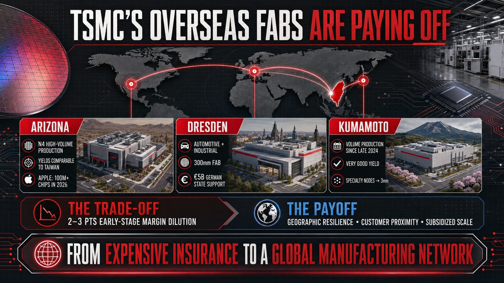

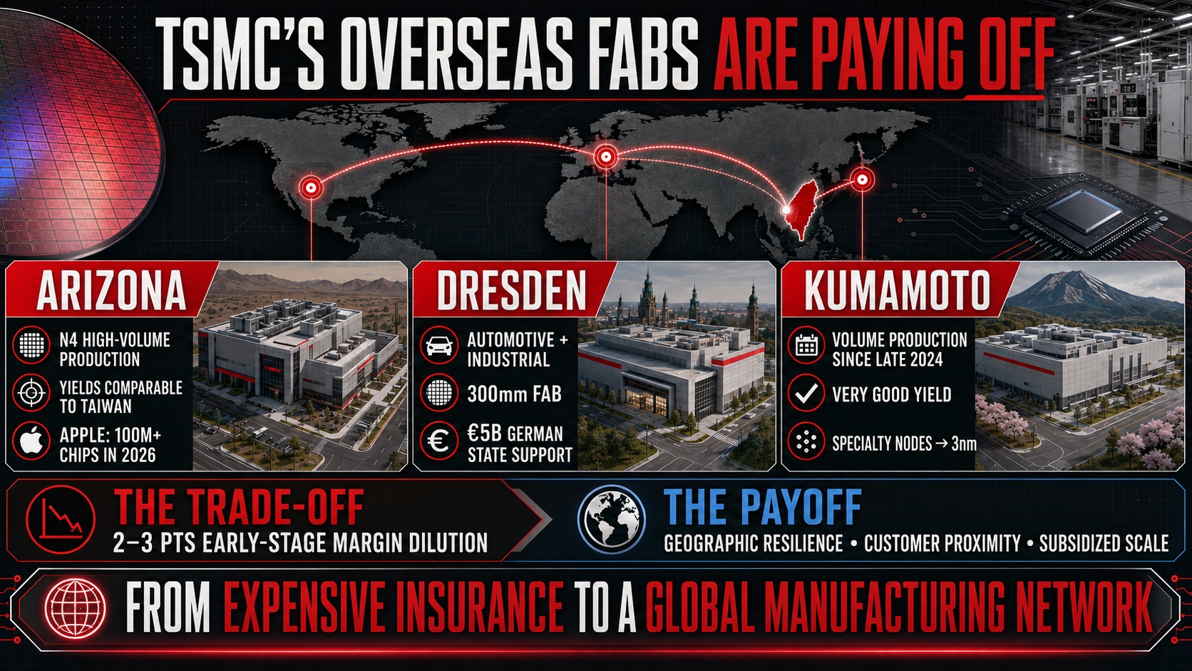
TSMC’s overseas fabrication strategy is beginning to deliver its intended return: not immediate cost parity with Taiwan, but manufacturable geographic redundancy, closer integration with major customers and access to subsidized capacity in strategically important markets. Arizona and Kumamoto are already producing commercially, while Dresden extends the model into Europe’s automotive semiconductor ecosystem.
The clearest validation is Arizona’s Fab 21. Its first phase entered high-volume production on the N4 process in the fourth quarter of 2024, achieving yields comparable with TSMC’s Taiwanese fabs. Yield parity matters because advanced-node economics are extremely sensitive to defect density. A foreign fab that requires substantially more wafer starts per functional die would provide political resilience but destroy economic value. Arizona has crossed that technical threshold.
Demand is also materializing. Apple, the fab’s first and largest customer, expects to purchase well over 100 million advanced chips from the facility in 2026—a significant increase from 2025. AMD has likewise identified Arizona as a source of leading-edge products. TSMC has therefore accelerated its second Arizona fab, now scheduled for high-volume manufacturing in the second half of 2027. That facility will introduce 3-nanometer-class production, while subsequent fabs are planned for N2, A16 and later technologies. The objective is no longer an isolated factory; it is an independent “GIGAFAB” cluster incorporating wafer fabrication, advanced packaging and research capabilities. (TSMC, Apple)
Kumamoto demonstrates a complementary localization model. Japan Advanced Semiconductor Manufacturing, TSMC’s venture with Sony, Denso and Toyota, began volume production in late 2024 with what TSMC describes as very good yield. Its initial 12/16-nanometer and 22/28-nanometer processes serve image sensors, automotive controllers and industrial devices—markets where supply continuity, qualification history and proximity to customers can be more valuable than transistor density. A second Kumamoto fab is under construction, and TSMC now plans to introduce 3-nanometer technology there in response to AI-related demand. This converts Japan from a specialty-node outpost into a potential advanced-logic base.
Dresden completes the regional segmentation. European Semiconductor Manufacturing Company, owned by TSMC, Bosch, Infineon and NXP, is designed around 300-millimeter automotive and industrial production rather than leading-edge AI accelerators. Its technology portfolio and local joint-venture structure reduce qualification and logistics risks for European customers. Germany’s €5 billion state-aid package offsets part of the structural cost disadvantage of manufacturing in Europe. (European Commission)
The payoff should not be confused with near-term margin accretion. Labor, construction, utilities, supplier density and smaller initial scale make overseas wafers more expensive. TSMC forecasts that foreign-fab ramp-ups will dilute gross margin by two to three percentage points in their early stages and by three to four points later as expansion accelerates. Nevertheless, the company posted a 59.9% gross margin in 2025, suggesting that leading-edge demand, utilization and pricing can absorb the burden. (TSMC Q2 2026)
Bottom Line: The strategic return is therefore risk-adjusted rather than purely accounting-based. Subsidies lower capital intensity; customer commitments improve utilization visibility; replicated process control proves that TSMC’s manufacturing system can travel; and regional capacity reduces exposure to earthquakes, shipping disruptions and geopolitical concentration. Taiwan will remain the center of TSMC’s newest technology and largest scale. But overseas fabs are evolving from expensive insurance policies into productive, customer-backed nodes of a global manufacturing network—and that is precisely how the investment begins to pay off.
Also Read:
How TSMC Is Wiring the AI Era With Light
A 0.42-Nanometer Breakthrough From TSMC Could Push Transistors Beyond Silicon
Intel and TSMC Take Different Paths to High-NA EUV
Share this post via:



Comments
There are no comments yet.
You must register or log in to view/post comments.