




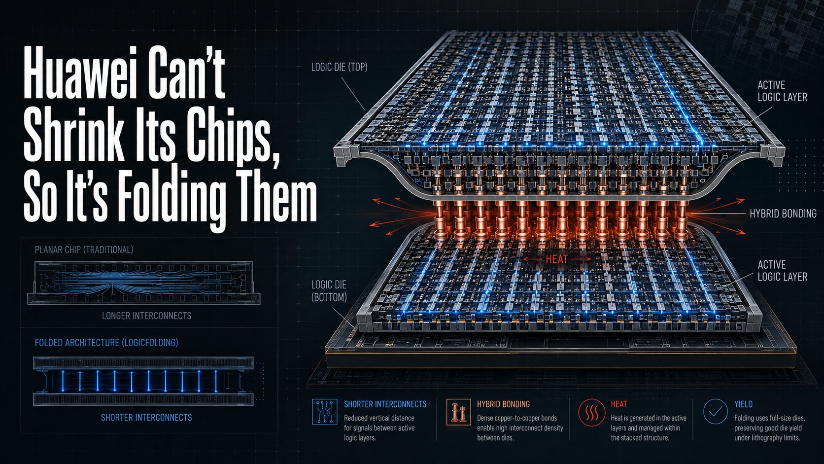



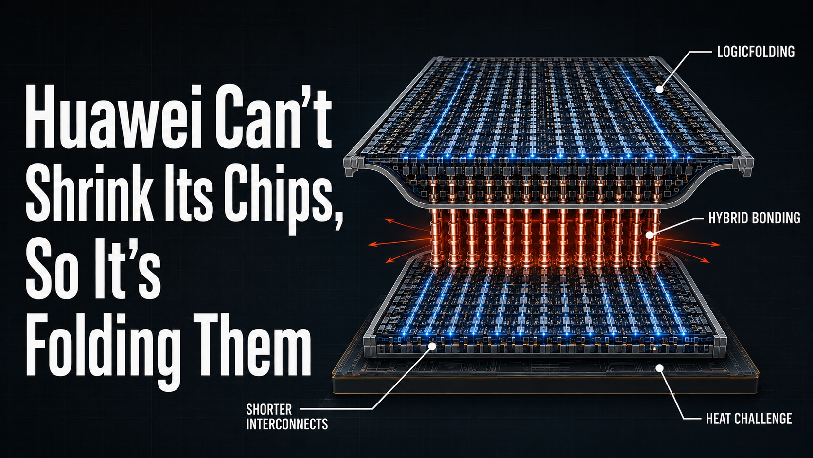
On May 25, Huawei semiconductor chief He Tingbo unveiled LogicFolding, an architecture intended to advance chip performance without relying on ever-smaller transistors. Presented alongside Huawei’s “Tau Scaling Law,” the approach prioritizes signal speed over transistor dimensions. It is a genuine engineering response to U.S. export controls—but Huawei’s ambitious claims still face formidable obstacles involving heat, manufacturing yield, and design software.
For decades, semiconductor progress has depended on shrinking transistors. Huawei can no longer follow that path easily. U.S. restrictions have blocked Chinese access to ASML’s extreme-ultraviolet lithography systems and leading-edge manufacturing at TSMC. China’s top foundry, SMIC, currently produces 7-nanometer-class chips through costly deep-ultraviolet multi-patterning, repeatedly exposing the same layers. Each additional exposure raises production costs and the risk of defects. SMIC’s developing 5-nanometer-class process may cost 40 to 50 percent more than TSMC’s equivalent.
LogicFolding seeks to compensate by reorganizing the chip. Rather than making components smaller, Huawei stacks two active layers face to face, bringing circuits that would ordinarily sit far apart into close proximity. Tingbo He’s paper describes distributing digital, analog, and memory circuits among vertically connected tiers using hybrid bonding. Shorter connections can reduce delays and energy consumption. Huawei claims the resulting architecture increases transistor density by 55 percent and improves power efficiency by 41 percent.
Those figures require careful interpretation. LogicFolding’s gains arise largely from shortening wires and using space vertically, not from manufacturing smaller transistors. Huawei’s goal of achieving density “equivalent to 1.4 nanometers” by 2031 therefore does not mean it will possess a genuine 1.4-nanometer fabrication process. TSMC’s actual A14 process is scheduled for volume production in 2028—three years before Huawei hopes to attain comparable density through stacking.
Huawei must also overcome two serious technical barriers. The first is heat. Stacking active logic layers makes it harder to remove thermal energy, potentially reducing performance and reliability. He has acknowledged that thermal management remains a central challenge. The second is yield. Defects compound when multiple layers are bonded: if each tier has a 50 percent yield, only roughly 25 percent of completed two-tier devices may be usable. With SMIC’s reported 5-nanometer yields already far below TSMC’s, stacking could amplify an existing cost disadvantage.
The software toolchain presents another bottleneck. Designing true three-dimensional chips requires electronic design automation software capable of placing components, routing signals, modeling heat, and verifying performance across tiers. American companies dominate this industry and are subject to export controls. Peking University has developed a prototype tool tailored to LogicFolding, but transforming an academic system into production-grade software may take years. Huawei itself identifies the toolchain as the most important enabling investment for the coming decade.
The first meaningful test may arrive this fall, when Huawei’s Kirin 9050 is expected to appear in the Mate 90 smartphone. Independent benchmarks could show whether LogicFolding’s promised gains survive commercial manufacturing and sustained operation. Huawei also plans to extend folding to its Ascend AI accelerators around 2030, where power density and cooling will pose even greater challenges.
Bottom line: LogicFolding demonstrates that export controls can redirect innovation rather than stop it. Yet it also reveals their impact: Huawei is pursuing a more complex, expensive, and yield-sensitive route because conventional scaling has been closed off. Washington should maintain controls on EUV technology, examine dependencies in advanced packaging equipment and specialty chemicals, and invest in American research on three-dimensional integration. Huawei has found a creative detour, but whether it becomes a commercially viable highway remains uncertain.
Also Read:
A 0.42-Nanometer Breakthrough From TSMC Could Push Transistors Beyond Silicon
Intel and TSMC Take Different Paths to High-NA EUV
White Paper: The Semiconductor Foundation of Modern AI Data Centers
Share this post via:



Intel Foundry: AI performance now depends on the whole system