





Why Advanced-Node Clock Networks Need More Than Timing Closure
Timing closure has been one of the semiconductor industry’s most reliable measures of design readiness for decades. Static timing analysis (STA) is a critical enabler for this process. It allows analysis of enormous designs across millions of paths, multiple modes, process corners, voltages, and temperatures with extraordinary efficiency.
But as technology advances, a timing-clean clock network can leave important questions unanswered about power, jitter, duty cycle, aging, margin, and ultimately silicon behavior. The issue is not that STA has stopped working. The question is whether timing closure alone still tells us enough about the electrical behavior of the clock network.
At older process nodes, there was often enough margin to absorb modeling uncertainty and electrical effects that could reasonably be treated separately. At 5nm, 3nm, 2nm and below, that cushion is getting smaller. Supply voltages are lower, interconnect effects are larger, power delivery has become more challenging, and a few picoseconds can materially affect design outcomes.
These trends suggest the end of “good enough” timing analysis. Let’s look closer.
Timing Closure and Clock Understanding Are Not the Same Thing
A clock network can meet its timing requirements and still leave important engineering questions such as these unanswered:
- How much of the reported clock margin is physically required?
- How much jitter accumulates from the clock source to the sequential endpoint?
- How does supply noise affect clock behavior across the complete distribution network?
- Is clock power higher than necessary?
- How does duty-cycle distortion propagate through multiple stages?
- How will aging affect the clock over the lifetime of the product?
- Are these effects independent, or are they interacting?
- Could a change that improves one metric make another worse?
These are not theoretical questions. A clock network is not simply a collection of timing paths. It is a distributed electrical system.
A design change made to improve one metric can influence several others. Upsizing a clock cell may improve slew, but it can also increase power and local supply disturbance. Downsizing may reduce power while changing delay, jitter sensitivity, and duty-cycle behavior. Supply variation can become timing variation. Jitter introduced near the clock source can propagate and accumulate through the entire distribution network.
A timing report can tell an engineer whether the required constraint was met, but it may not disclose everything about why the clock behaved that way.
Solving Complexity Through Abstraction
This is not an argument against abstraction. Modern semiconductor design would be impossible without it. STA solves timing at tremendous scale. Power integrity tools analyze supply behavior. Jitter methodologies account for clock uncertainty. Aging models estimate lifetime degradation. Variation methodologies account for process and operating uncertainty.
Each of these approaches solves a necessary problem. The challenge is that silicon does not experience these effects one at a time. When a physical system is decomposed into separate analyses, each methodology must make assumptions about the effects being handled elsewhere, and those assumptions are appropriately designed to protect against failure.
As design margins tighten, however, it becomes increasingly valuable to understand how those effects interact electrically across the complete clock network. This is especially important for clocks because the same signal propagates through many stages and ultimately reaches a very large number of sequential endpoints. Small differences that appear insignificant locally can accumulate across the network.
More Margin Is Not More Understanding
When uncertainty exists, designers add margin. That is rational engineering. But margin is not free. Additional clock margin can translate into lower frequency, higher operating voltage, increased power, larger cells, more buffering, reduced thermal headroom, or less flexibility elsewhere in the design. The important question is therefore not whether margin should exist.
The more useful question is: How much of that margin is required by the electrical behavior of the clock, and how much is protecting against what the methodology cannot directly see?
This distinction becomes increasingly important when timing, voltage sensitivity, jitter, aging, duty cycle, and other effects are evaluated separately. The goal is not simply to remove margin. It is to understand it well enough to make better margin decisions. That difference matters.
Timing is Closed, but is the Clock Optimized?
Once timing closes, optimization raises a different set of questions, such as:
- Could the clock network meet its requirements with less power?
- Are some clock cells over-driven?
- Is a particular domain carrying more margin than its electrical behavior requires?
- Is jitter consuming meaningful timing headroom?
- Is duty-cycle distortion creating risk on half-cycle paths or memories?
- Will aging materially change the behavior over product lifetime?
A clock network can be timing-clean and still contain opportunities for improved power, performance, robustness, or margin.
This is particularly important in high-performance designs such as those powering AI workloads, where both power and frequency are under intense pressure. A few picoseconds of unnecessary clock margin or a small amount of excess clock power may appear insignificant in isolation, but those costs scale across large designs and persist for every operating cycle.
Timing closure is therefore an important milestone. It does not necessarily mean the clock is finished, however.
The Missing Piece: Electrical Context
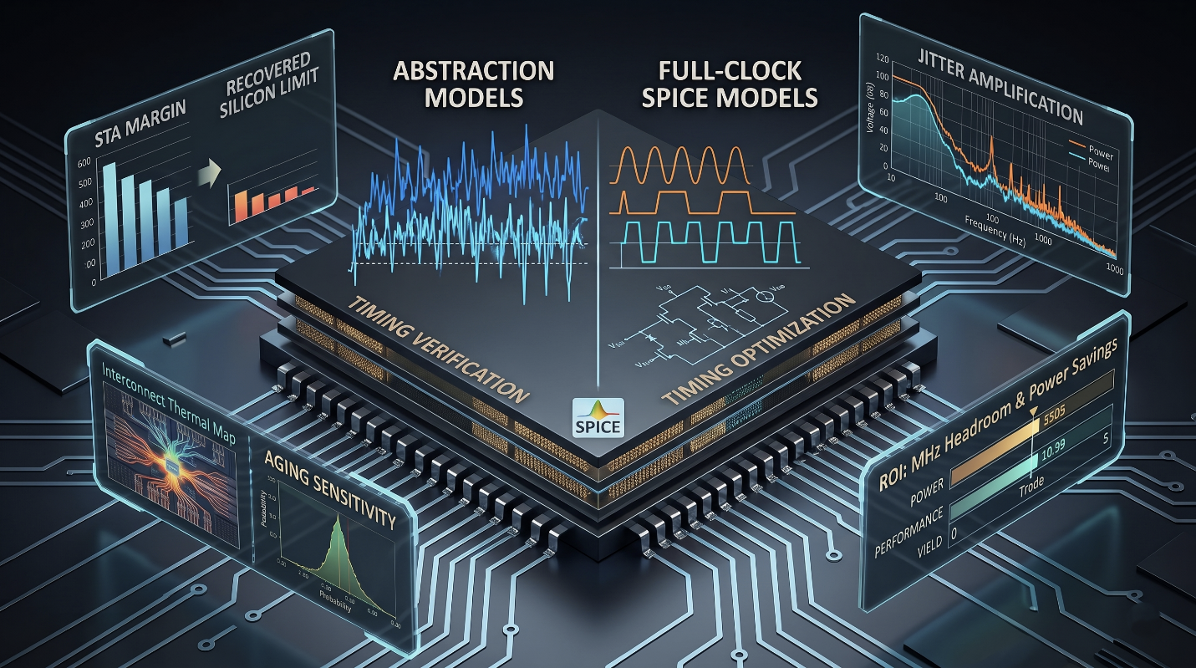
What advanced-node clock design increasingly needs is not a replacement for STA. It needs a complementary level of electrical visibility.
Imagine being able to examine the clock from its PLL or source through the complete distribution network to sequential endpoints and see how timing, jitter, power, duty cycle, supply sensitivity, and aging develop across that system. That changes the nature of the engineering discussion.
Instead of only asking whether a constraint has been met, engineers can ask:
- Where is the limitation originating?
- Is the behavior local or cumulative?
- Which operating condition is controlling the result?
- Which design change will produce the greatest benefit?
- Can power be reduced without compromising clock integrity?
- Can margin be refined while maintaining sign-off confidence?
These are optimization questions, not verification questions. Answering them requires understanding the electrical behavior behind the report. Historically, however, there has been a practical barrier to obtaining that level of visibility across an entire SoC clock network: SPICE accuracy came with a capacity and runtime penalty.
Design teams therefore made a sensible tradeoff. Detailed transistor-level analysis was applied where electrical accuracy was essential, while abstraction provided the capacity required for large-scale analysis.
That tradeoff is beginning to change.
Distributed computing and advances in simulation are making SPICE-accurate electrical analysis practical for complete clock networks at SoC scale and within usable engineering runtimes. This makes it possible to examine the clock as the connected electrical system it actually is – from the PLL or clock source through the distribution network to sequential endpoints.
Instead of examining timing, jitter, power, duty cycle, supply sensitivity, and aging only through separate abstractions, engineers can add a full-network electrical view. And once that level of analysis becomes practical, there is no reason to reserve it only for the end of the flow.
Electrical insight can be introduced around clock tree synthesis, when implementation choices can still be changed, and carried through sign-off and into silicon correlation.
Moving Beyond “Good Enough”
STA will remain fundamental to semiconductor design because nothing else provides its extraordinary combination of capacity, coverage, and efficiency. What may be reaching its limit is the assumption that timing closure alone is a sufficient proxy for understanding the electrical behavior of the clock network.
That shift – from simply verifying the clock to understanding its electrical behavior – is the opportunity.
ClockEdge® is a company that addresses the needs discussed here. It provides scalable, SPICE-accurate analysis of complete clock networks, from the PLL or clock source to sequential endpoints, across timing, power, jitter, duty cycle, aging, sensitivity, and optimization. Its distributed architecture enables full-network electrical analysis within practical engineering runtimes. You can learn more about this important company here.
The goal is not to replace timing closure. It is to know more once you get there.
That’s what the end of “good enough” timing analysis looks like.
Also Read:
What is the 3nm Pessimism Wall and Why is it An Economic Crisis?
The Risk of Not Optimizing Clock Power
Taming Advanced Node Clock Network Challenges: Jitter
Share this post via:



Comments
There are no comments yet.
You must register or log in to view/post comments.