







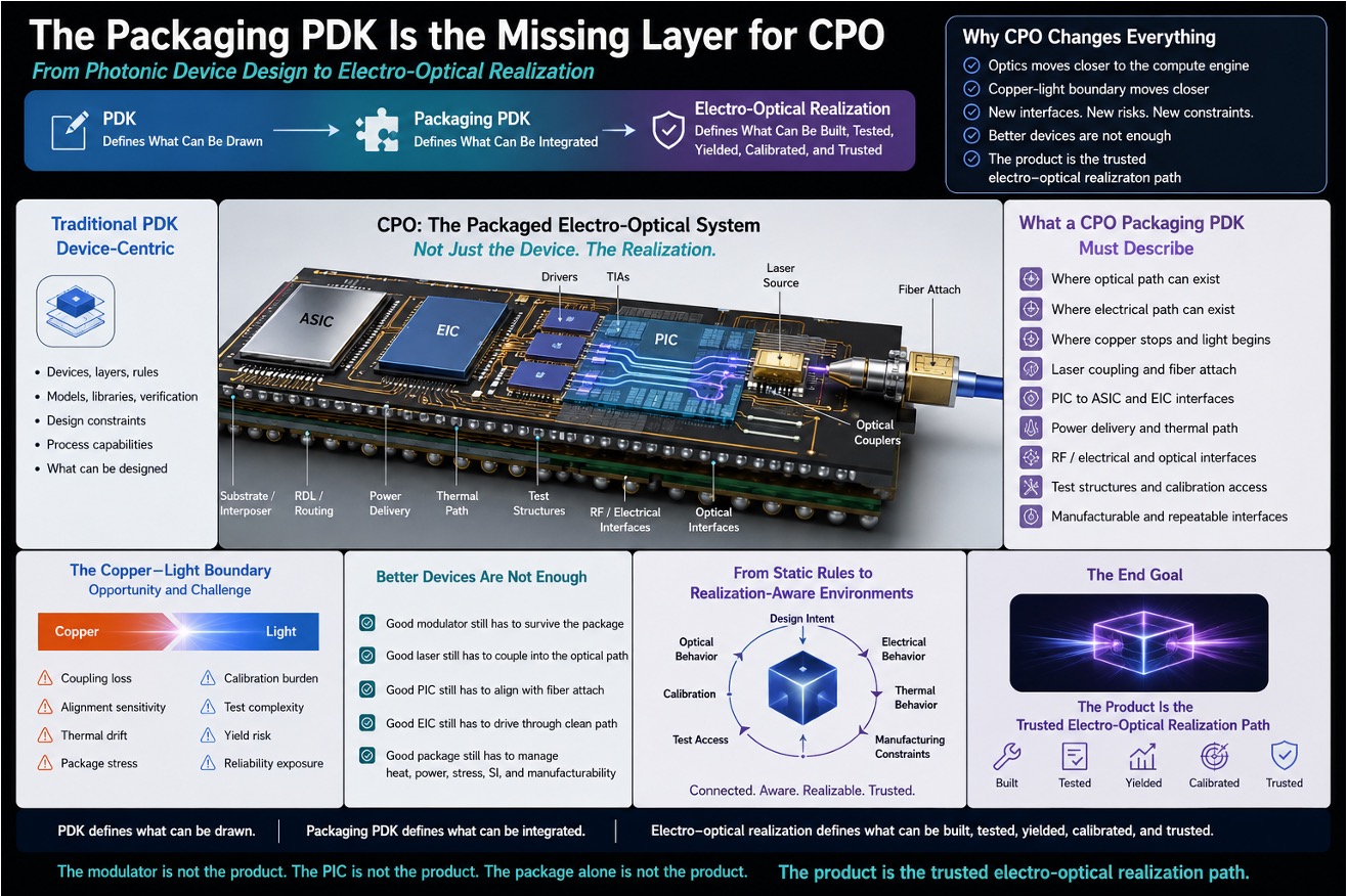
From Photonic Device Design to Electro-Optical Realization
Co-packaged optics will not scale through photonic device performance alone.
As AI infrastructure pushes bandwidth, power, latency, and reach to new limits, optics is moving closer to the compute engine. The industry is no longer asking only whether a photonic device can operate at high speed. It is asking whether the full electro-optical path can be designed, packaged, powered, cooled, tested, calibrated, manufactured, and trusted at scale.
That shift changes the meaning of a PDK.
For CPO, the PDK must evolve from a device-design kit into a realization interface kit.
The Traditional Role of the PDK
In traditional semiconductor design, a process design kit defines what can be designed, manufactured, modeled, checked, and trusted within a process.
It gives engineers rules, devices, layers, design constraints, models, extraction views, and verification hooks. It allows a design team to move from design intent to manufacturable silicon with a shared understanding of what is allowed, what is characterized, what is checked, and what the foundry process can support.
The PDK is not only a convenience file set.
It is a contract between design and manufacturing.
It defines the design space that can be realized with confidence.
That concept becomes even more important as semiconductor systems move from monolithic silicon to heterogeneous integration, chiplets, advanced substrates, high-bandwidth memory, optical I/O, and co-packaged optics.
CPO Changes the Meaning of the PDK
Optical co-packaging changes the design problem.
For CPO, the product is not only the photonic device.
It is the packaged electro-optical system.
A modulator, photodetector, laser interface, or waveguide may be excellent as an individual device, but that does not guarantee the final product can be built, tested, calibrated, and deployed.
The design kit cannot stop at the PIC layout or optical device library.
It must begin to describe the interfaces among:
PIC
ASIC
EIC
drivers
TIAs
SerDes
laser source
fiber attach
waveguides
couplers
interposer
substrate
RDL
power delivery
thermal path
RF / electrical interface
optical interface
test structures
calibration access
This is why packaging PDKs may become one of the most important missing links for CPO.
The Packaging PDK as a Realization Contract
A CPO packaging PDK is not just a file set.
It is a realization contract.
It should help define where the optical path can exist, where the electrical path can exist, where copper stops and light begins, how the laser is coupled, how the fiber is attached, how the PIC connects to the ASIC, how heat is removed, how power is delivered, how RF and optical interfaces are tested, how alignment and loss are controlled, and which package interfaces are manufacturable and repeatable.
That is a different level of abstraction than a conventional device PDK.
A photonic device PDK may tell the designer how to draw a waveguide, modulator, grating coupler, photodetector, or routing structure.
A packaging PDK for CPO must help describe whether that optical function can survive the package.
It must connect optical behavior to package interfaces, thermal behavior, mechanical stress, electrical drive conditions, fiber attach, calibration, test access, and manufacturability.
For CPO, the package is not passive.
The package becomes the place where the optical, electrical, thermal, mechanical, and manufacturing domains converge.
The Copper-Light Boundary
CPO is not simply about moving optics closer to the ASIC.
It is about moving the copper-light boundary closer to the compute engine.
That boundary is not free.
Electrical signals over copper face reach, loss, crosstalk, impedance discontinuity, equalization power, and heat challenges as bandwidth and distance increase.
Optics can improve communication reach and bandwidth density, but optical integration introduces its own boundary burden.
That burden includes coupling loss, alignment sensitivity, thermal drift, package stress, calibration requirements, optical test complexity, manufacturing variability, and reliability exposure.
This is why CPO cannot be evaluated only by the performance of an optical device.
The system must evaluate the boundary itself.
Where does copper stop?
Where does light begin?
How is the optical path coupled?
How is the electrical path driven?
How is the thermal path controlled?
How is alignment maintained?
How is calibration performed?
How is the optical interface tested?
How is stability proven over time?
These are not only design questions.
They are realization questions.
Better Devices Are Not Enough
The industry needs better photonic devices.
But better photonic devices alone are not enough.
A good modulator still has to survive the package.
A good laser still has to couple into the optical path.
A good PIC still has to align with fiber attach.
A good EIC still has to drive the optical device through a clean electrical path.
A good package still has to manage heat, power, stress, signal integrity, manufacturability, and test access.
This is where packaging PDKs become strategic.
They move CPO from a device-level design problem toward a system-level realization problem.
The question is no longer only:
Can the optical device work?
The harder question is:
Can the packaged electro-optical path be built, tested, calibrated, yielded, and trusted at scale?
What a CPO Packaging PDK Should Enable
A useful packaging PDK for CPO should not be limited to physical layout constraints.
It should help connect the critical interfaces that determine whether optical co-packaging can become a repeatable product.
That includes optical interface definition, electrical interface definition, mechanical keep-out regions, fiber attach constraints, substrate and interposer interface rules, thermal path awareness, package-level design limits, test structure planning, calibration access, and manufacturability guidance.
It should help engineering teams understand not only what can be drawn, but what can be integrated.
In that sense, the packaging PDK becomes a bridge between the photonic device design space and the packaged system realization space.
For example, the PDK should help answer questions such as:
Where can optical routing exist inside the package?
What optical coupling structures are supported?
What fiber attach approaches are compatible with the package?
What electrical drive paths are allowed between the EIC and PIC?
What thermal constraints affect optical stability?
What package-level stress conditions may affect optical alignment?
What test structures are needed for optical and electrical validation?
What calibration access is required after assembly?
Which interfaces are mature enough for repeatable manufacturing?
These questions are not separate from the product.
They define the product.
From Static Rules to Realization-Aware Environments
The next step is even bigger.
As CPO matures, static rules will not be enough.
The industry will need realization-aware environments that connect design intent, package interfaces, optical behavior, electrical behavior, thermal behavior, manufacturing constraints, test access, calibration, and lifecycle reliability.
This does not mean every PDK must become a full system simulator.
It means the boundary between device design, package design, test, and manufacturing must become more connected.
A realization-aware packaging PDK should help prevent the common failure mode where the device looks good, the package looks good, and the system still fails at the interface.
That interface is where CPO succeeds or fails.
The optical path, electrical path, thermal path, mechanical structure, and test strategy must be developed as one integrated realization problem.
Why This Matters for AI Infrastructure
AI infrastructure is increasingly constrained by data movement.
Moving data between accelerators, memory, switches, racks, and clusters drives power, latency, thermal load, bandwidth limitations, and system cost.
That is why optical I/O and CPO are receiving so much attention.
But AI infrastructure does not need beautiful optical devices alone.
It needs deployable optical communication systems.
A data center cannot operate on record-setting lab performance. It needs manufacturable modules, stable coupling, reliable attach, controlled thermal behavior, test coverage, calibration flows, field diagnostics, and supply-chain repeatability.
This is where packaging PDKs can become a key enabler.
They can help convert optical innovation into packaged system realization.
The New PDK Hierarchy
The industry may need to think about a broader hierarchy:
PDK defines what can be drawn.
Packaging PDK defines what can be integrated.
Electro-optical realization defines what can be built, tested, yielded, calibrated, and trusted.
This is the path from photonic device design to deployable AI photonics infrastructure.
The modulator is not the product.
The PIC is not the product.
The package alone is not the product.
The product is the trusted electro-optical realization path.
Conclusion
Co-packaged optics represents more than a new placement of optical engines.
It represents a change in how the semiconductor industry must define design readiness, package readiness, test readiness, and manufacturing readiness for electro-optical systems.
A conventional photonic PDK can help create the device.
A packaging PDK can help create the interface.
A realization-aware environment can help create the product.
For CPO, the packaging PDK may become the missing layer between photonic device innovation and AI infrastructure deployment.
The next phase of CPO will not be won by optical performance alone.
It will be won by the teams that can define, integrate, test, calibrate, manufacture, and trust the full electro-optical realization path.
Also Read:
The Modulator Is Not the Product: Why AI A tower-like heterogeneous packaging architecture for the AI era
Photonics Needs an Electro-Optical Realization Corridor
From Evidence to Authority: Bounded Gate Authority for Governed Semiconductor Realization
Share this post via:



Terafab’s Single Roof: Why Packaging, Not Lithography, Decides High Volume