




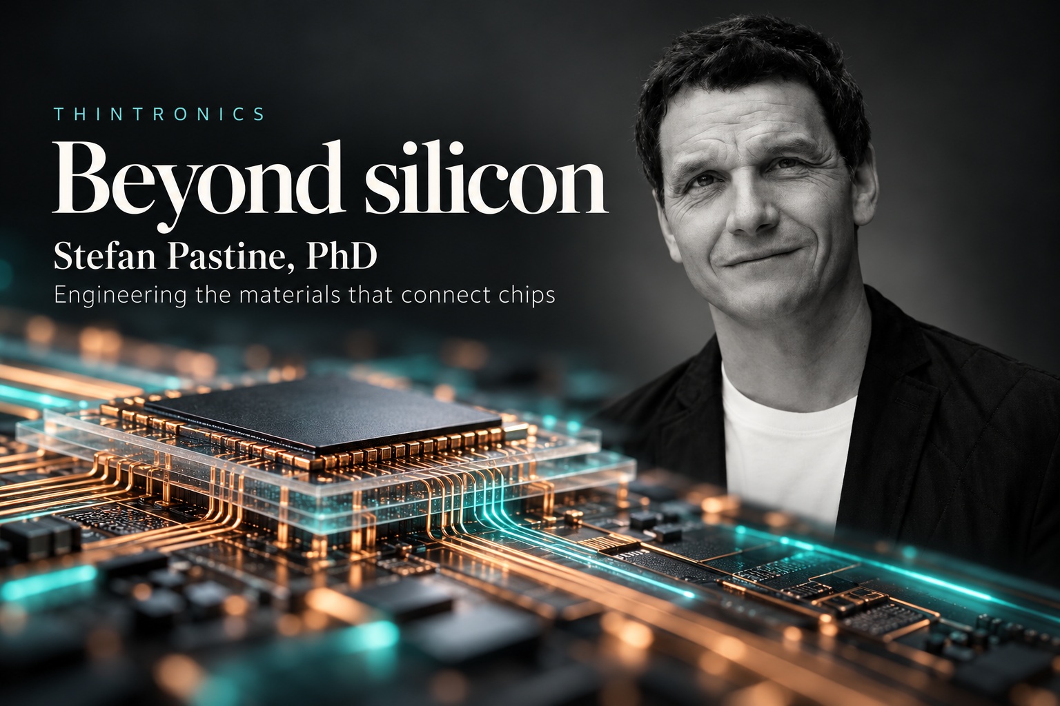



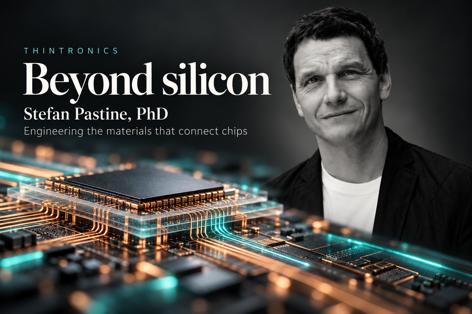
Stefan Pastine PhD is an American chemist and entrepreneur. In 2011, he founded Connora Technologies, developer of Recyclamine, a recyclable epoxy thermoset technology that allows carbon fiber, fiberglass, and aramid fiber to be recovered from composite waste. Aditya Birla Chemicals acquired Connora in 2019 and applied the technology to recyclable wind turbine blades.
Pastine founded Thintronics in 2019, developing polymer-based materials that improve signal integrity and reduce thermal resistance in high-performance computing, including AI, data centers, and networking. Thintronics closed a $20 million Series A in 2024 and is now negotiating a $50 million CHIPS Act award. The company is based in the San Francisco Bay Area.
Tell us about your company?
Thintronics is an advanced materials company focused on a growing semiconductor bottleneck: the materials connecting chips.
As data rates move from 224G toward 448G, the physics of the package becomes increasingly important. Signal loss, power consumption and heat are being constrained by dielectric materials that were developed for a very different performance era.
Thintronics was founded to change that. We develop ultra-low-loss dielectric technology for advanced semiconductor packaging, engineering materials from the molecular level through to system-level electrical performance.
The larger story is that semiconductor performance can no longer be driven by silicon alone. Increasingly, what surrounds and connects the chip determines what the chip can actually do. That’s the problem Thintronics was built to solve.
What problems are you solving?
Two, and they compound each other. The first is physics: as the industry pushes from 224G toward 448G, the dielectric materials inside every chip substrate (managing heat, signal loss, and power) are running into real limits. These materials were engineered for a much slower era, and they’re now the bottleneck standing between the chip and the performance it’s actually capable of.
The second is structural, and it’s the one people find more surprising: virtually the entire industry sources this material from a single supplier, based in Japan. That’s the exact same single-point-of-failure dynamic that shut down auto plants during COVID, except this time it sits at the center of the semiconductor supply chain, not the edge of it. Solving the physics without solving the supply chain risk doesn’t really solve the problem. We’re solving both at once.
What application areas are your strongest?
AI infrastructure is the sharpest edge of this problem right now. AI accelerators and the networking that ties them together are pushing data rates harder and faster than almost anything else in the industry, which means they hit the dielectric performance ceiling first. That’s where we’re seeing the most urgent pull, hyperscale AI packaging, high-speed networking, and next-gen ASICs, anywhere the interconnect itself has become the constraint rather than the chip. The same physics problem shows up in high-performance computing and advanced RF/mmWave systems too, so the material has legs beyond any single application, but AI is where the pain is most acute today, and where we’ve focused first.
What keeps your customers up at night?
Two things, and they’re in tension with each other. First, roadmap risk: their next-generation packages are designed around performance targets that the incumbent material can’t hit, and there’s no easy substitute sitting on the shelf. Second, supply risk: even the material they’re using today runs through one supplier, so any disruption, whether geopolitical, logistical, anything, is a single point of failure sitting at the center of their entire product line. Customers are being asked to hit performance targets and de-risk their supply chain at the same time, with the same incumbent material failing them on both fronts. That’s the anxiety we hear in almost every conversation.
What does the competitive landscape look like and how do you differentiate?
The obvious competitors are the American domestic majors — 3M, Rogers, Isola — who are building their own build-up film alternatives, and that’s a healthy sign in itself: it confirms this bottleneck is real and worth solving, not something we invented. But building a better film in isolation isn’t the hard part of this problem.
Where Thintronics differentiates is vertical integration, and specifically the kind that’s hard to replicate outside Silicon Valley. We’re not just a chemistry company that happens to sell into semiconductors, we’ve built a team that spans chemists developing the material at the molecular level, mechanical engineers who understand how it behaves under real thermal and mechanical stress, and electrical engineers and designers who have shipped real substrates into production. That means we’re not handing a datasheet to a customer and hoping it fits their system. We can solve problems at every bottleneck in the value chain — material, process, and system-level performance — because the people solving each one are sitting in the same room.
That’s the real differentiation: the incumbents and the domestic majors are optimizing one layer of the stack. We’re built to optimize the whole path from molecule to shipped product.
What new features/technology are you working on?
Right now, the dielectric materials across a single package are a patchwork of different materials at the PCB, substrate, and interposer layers, each with different electrical and mechanical performance, often from different suppliers who weren’t designing with each other in mind. That heterogeneity is its own hidden cost: every interface between those materials is a place where performance leaks out and reliability risk creeps in.
Our roadmap is to fix that at the root. We’re developing a unified dielectric system that spans the entire stack, PCB, substrate, and interposer, built from the same underlying material platform rather than stitched together from whatever each layer’s incumbent supplier happens to offer. That means a customer isn’t just solving today’s bottleneck; they’re moving toward a package where every layer speaks the same electrical and mechanical language, engineered together instead of independently. It’s also appealing to designers to be able to work with the whole stack in mind.
How do customers normally engage with your company?
With fabless design teams, we start with the packaging and signal integrity engineers, working through how the material improves their existing channel and where it fits into what they’ve already built. If that constraint genuinely lifts, it opens the door to a bigger conversation with the architecture team about system-level improvements that weren’t possible before. From there, we review the actual design files and build with a qualified fab, then move into assembly.
With factories, the relationship runs differently, because it’s less about the material itself and more about how it behaves inside their specific process and economics. We bring deep domain understanding of factory processes to the table, along with customer designs the factory can actually run efficiently. Qualification happens with our guidance on process integration, and in many cases we embed a field applications engineer with real fab knowledge directly at the customer’s site to help dial in the process.
With OSATs, who are typically helping lower-volume customers design and procure substrates, we engage by providing reference designs and blocks the factory can build directly — which has the added benefit of helping anchor volume at the fab. From there, the engagement mirrors what we do with fabless teams directly.
So it’s really three different front doors into the same underlying discipline: understand where the material has to prove itself first, then work inside whichever design and manufacturing relationship the customer already has, rather than asking them to change how they operate to accommodate us.
Also Read:
Executive Interview with Raghu Belur, Co-Founder of Enphase Energy
CEO Interview with Charlie Cheng of CEO of TeRAM
SemiWiki CEO Interview with Dr. Nissan Maskil of Qarakal Quantum
Share this post via:



Terafab’s Single Roof: Why Packaging, Not Lithography, Decides High Volume