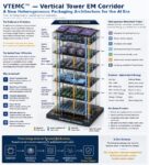
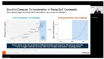
For years, advanced packaging has been described mostly in planar terms: chiplets placed side by side, connected through interposers, bridges, redistribution layers, substrates, and short-reach electrical links. This view remains important. It supports today’s GPU, HBM, chiplet, and 2.5D integration architectures.… Read More
Tag: hbm
From Evidence to Authority: Bounded Gate Authority for Governed Semiconductor Realization
Advanced semiconductor systems are no longer limited by a single engineering domain. They are constrained by the convergence of many interdependent vectors: silicon nodes, advanced packaging architectures, substrate materials, platform PCBs, power-delivery networks, thermal behavior, manufacturing variation, firmware… Read More
What Winemakers and Chip Designers Have in Common
Consider this a standout presentation at the Silicon Catalyst Spring Portfolio Update Meeting held yesterday at the Computer History Museum. Mahesh Tirupattur, CEO of Analog Bits, is a modern-day, multidimensional semiconductor hero and one of my trusted few. Analog Bits is a premier member of the semiconductor ecosystem,… Read More
Scaling Multi-Die Connectivity: Automated Routing for High-Speed Interfaces
This article concludes the three-part series examining key methodologies required for successful multi-die design. The first article Reducing Risk Early: Multi-Die Design Feasibility Exploration focused on feasibility exploration and early architectural validation, while the second article Building the Interconnect… Read More
Arteris Smart NoC Automation: Accelerating AI-Ready SoC Design in the Era of Chiplets
As semiconductor design pushes into increasingly complex territory, driven by Ai, ML, HPC, and heterogeneous system architectures, designers are challenged to balance performance, power, and time-to-market pressures. In this landscape, network-on-chip (NoC) architectures have emerged as a foundational building block… Read More
Signal Integrity Verification Using SPICE and IBIS-AMI
High-speed signals enable electronic systems by using memory interfaces, SerDes channels, data center backplanes and connectivity in automobiles. Challenges arise from signal distortions like inter-symbol interference, channel loss and dispersion effects. Multi-gigabit data transfer rates in High-Bandwidth Memory… Read More
eBook on Mastering AI Chip Complexity: Pathways to First-Pass Silicon Success
The rapid evolution of artificial intelligence (AI) is transforming industries, from autonomous vehicles to data centers, demanding unprecedented computational power and efficiency. As highlighted in Synopsys’ guide, the global AI chip market is projected to reach $383 billion by 2032, growing at a 38% CAGR. This … Read More
Revolutionizing Chip Packaging: The Impact of Intel’s Embedded Multi-Die Interconnect Bridge (EMIB)
In an era dominated by artificial intelligence (AI), machine learning (ML), and high-performance computing (HPC), the demand for semiconductors that deliver high data throughput, low latency, and energy efficiency has never been greater. Traditional chip designs often struggle to keep pace with these requirements, leading… Read More
Synopsys Executive Forum: Driving Silicon and Systems Engineering Innovation
The annual SNUG (Synopsys Users Group) conference, now in its 35th year, once again brought together key stakeholders to showcase accomplishments, discuss challenges, and explore opportunities within the semiconductor and electronics industry. With approximately 2,500 attendees, SNUG 2025 served as a dynamic hub for collaboration… Read More
Evolution of Memory Test and Repair: From Silicon Design to AI-Driven Architectures
Memory testing in the early days of computing was a relatively straightforward process. Designers relied on simple, deterministic approaches to verify the functionality of memory modules. However, as memory density increased and systems became more complex, the likelihood of faults also rose. With advancements in memory… Read More
