You are currently viewing SemiWiki as a guest which gives you limited access to the site. To view blog comments and experience other SemiWiki features you must be a registered member. Registration is fast, simple, and absolutely free so please,
join our community today!
The annual SNUG (Synopsys Users Group) conference, now in its 35th year, once again brought together key stakeholders to showcase accomplishments, discuss challenges, and explore opportunities within the semiconductor and electronics industry. With approximately 2,500 attendees, SNUG 2025 served as a dynamic hub for collaboration… Read More
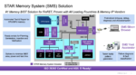
Memory testing in the early days of computing was a relatively straightforward process. Designers relied on simple, deterministic approaches to verify the functionality of memory modules. However, as memory density increased and systems became more complex, the likelihood of faults also rose. With advancements in memory… Read More
- QTR was just “in-line” but guide was below expectations
- We think its not just China export rules but share loss as well
- Leading edge is strong but obviously not enough to offset China
- Memory remains weak-Foundry (TSMC) is the primary driver
Headwinds slow growth to flat
Applied reported $7.166B in revenues and Non … Read More
– KLA put up a good qtr & year with consistent growth
– AI & HBM are the main drivers of leading edge which helps KLA
– China slowing but not too fast, Outlook OK but not super
– Wafer inspection is huge but reticle inspection continues to slip
KLA reports good quarter and OK outlook
KLA reported revenues… Read More
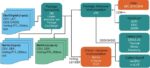
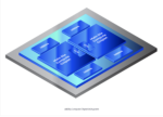
A growing trend in system design is the use of multiple ICs mounted in advanced packages, especially in high-performance computing and AI. These modern packages now integrate multiple ICs, often with high-bandwidth memory (HBM), resulting in hundreds of thousands of connections that need proper verification. Traditional… Read More
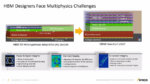
3D design with high-bandwidth memory stacks (HBM) has become essential for leading edge semiconductor systems in multiple applications. Hyperscalers depend on large AI accelerator cores supported by 100GB or more of in-package HBM to handle trillion parameter AI models. Autonomous Drive (AD) vehicles may handle smaller … Read More
- Consumer memory slowing more than AI gaining causing weakness
- HBM sold out for 2025- HBM is most of Capex- NAND near zero
- Big miss on Q1 guide crushes stock on disappointment
- Positive for Nvidia- Negative for Broadcom/Qualcomm
Micron – AI is wonderful & growing out of bounds while consumer sucks
Micron reported in line… Read More
Synopsys made significant announcements during the recent TSMC OIP Ecosystem Forum, showcasing a range of cutting-edge solutions designed to address the growing complexities in semiconductor design. With a strong emphasis on enabling next-generation chip architectures, Synopsys introduced both new technologies and … Read More
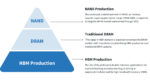
TechInsights has a new memory report that is worth a look. It is free if you are a registered member which I am. HBM is of great interest and there is a section on emerging and embedded memories for chip designers. Even though I am more of a logic person, memory is an important part of the semiconductor industry. In fact, logic and memory
…
Read More
Artificial intelligence (AI) and machine learning (ML) are evolving at an extraordinary pace, powering advancements across industries. As models grow larger and more sophisticated, they require vast amounts of data to be processed in real-time. This demand puts pressure on the underlying hardware infrastructure, particularly… Read More