You are currently viewing SemiWiki as a guest which gives you limited access to the site. To view blog comments and experience other SemiWiki features you must be a registered member. Registration is fast, simple, and absolutely free so please,
join our community today!
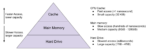
Memory Hierarchy and the Memory Wall
Computer programs mainly move data around. In the meantime, they do some computations on the data but the bulk of execution time and energy is spent moving data around. In computer jargon we say that applications tend to be memory bound: this means that memory is the main performance limiting … Read More
Wendy Chen, MBA from the University of Manchester, has been the Founder and CEO of MSquare Technology since 2021. With over 23 years in the semiconductor industry, Wendy’s career includes roles as Sales Director at Synopsys Technology, Vice President at TF-AMD, and Vice President at Alchip Asia Pacific. Her extensive experience… Read More
- AMAT reports good but underwhelming quarter
- China slowing creates revenue & GM headwinds- ICAPs weak
- AI remains the one and only bright spot in both foundry & memory
- Cyclical recovery remains slow – Single digit Y/Y growth
OK quarter – still slow growing, revs up only 5% Y/Y
AMAT came in at revenues of $6.78B… Read More
– We just finished the most happy SEMICON West in a long time
– IMEC stole the show- HBM has more impact than size dictates
– Has Samsung lost its memory mojo? Is SK the new leader?
– AI brings new tech issues with it – TSMC is still industry King
Report from SEMICON West
The crowds at Semicon West were both… Read More
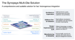
Introduction of 2.5D and 3D multi-die based products are helping extend the boundaries of Moore’s Law, overcoming limitations in speed and capacity for high-end computational tasks. In spite of its critical function within the 3DIC paradigm, the interposer die’s role and related challenges are often neither fully comprehended… Read More
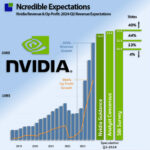
This article previews Nvidia’s earnings release and will be updated during and after the earnings release. As usual, we will compare and contrast the Nvidia earnings with our supply chain glasses to identify changes and derive insights. Please return to this article, as it will be updated over the next week as we progress with our… Read More
We are in the semiconductor market phase where everybody disagrees on what is going on. The market is up; the market is down. Mobile phones are up…. oh no, now they are down. The PC market is up—oh no, we need to wait until we can get an AI PC. The inflation is high—the consumer is not buying.
For us in the industry, the 13-week financial … Read More
– Lam reports another flat quarter & guide- No recovery in sight yet
– Seems like no expectation of recovery until 2025- Mixed results
– DRAM good- NAND weak- Foundry/Logic mixed-Mature weakening
– Clearly disappointing to investors & stock hoping for a chip recovery
Another Flat Quarter &
…
Read More
GenAI, the most talked-about manifestation of AI these days, imposes two tough constraints on a hardware platform. First, it demands massive memory to serve large language model with billions of parameters. Feasible in principle for a processor plus big DRAM off-chip and perhaps for some inference applications but too slow … Read More
MosChip is a publicly traded company founded in the year 1999, they offer semiconductor design services, turnkey ASIC, software services, and end-to-end product engineering solutions. The company headquartered in Hyderabad, India, with five design centers and over 1300 engineers located in Silicon Valley (USA), Hyderabad,… Read More