



1. Why the substrate matters
Every transistor sits in, or on, a few hundred nanometres of crystal; the rest of the wafer is mechanical support and, often, a liability. Silicon won because it combines a moderate bandgap (1.12 eV), a native oxide (SiO2) of excellent quality, and the ability to be grown as near-perfect single crystals at 300 mm diameter.
From the first planar ICs around 1960 until the 1990s, the industry scaled the transistor while treating the wafer mostly as a commodity, even though bipolar ICs already relied on epitaxial and buried layers, and the isolation problems SOI would later solve were known from the start. From the 1990s onward that assumption broke: parasitics, leakage and isolation problems rooted in the substrate began to limit speed, power and RF performance. The response was the engineered substrate, of which silicon-on-insulator (SOI) is the most successful example.
This tutorial follows that path: the bulk wafer, its limits, the SOI answer, its trade-offs, who makes it today, and where the field is heading.
2. The original structure: the bulk silicon wafer
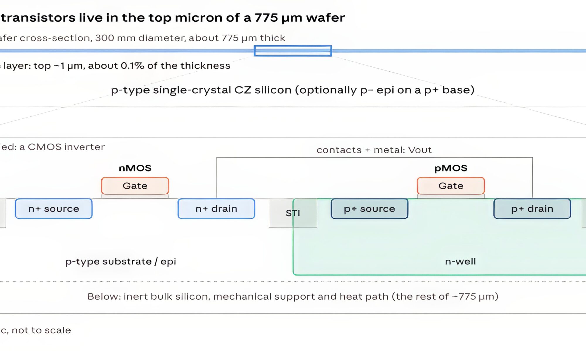
A bulk wafer is a single slab of doped crystalline silicon, about 775 µm thick at 300 mm, with devices built only in its top micron or so.
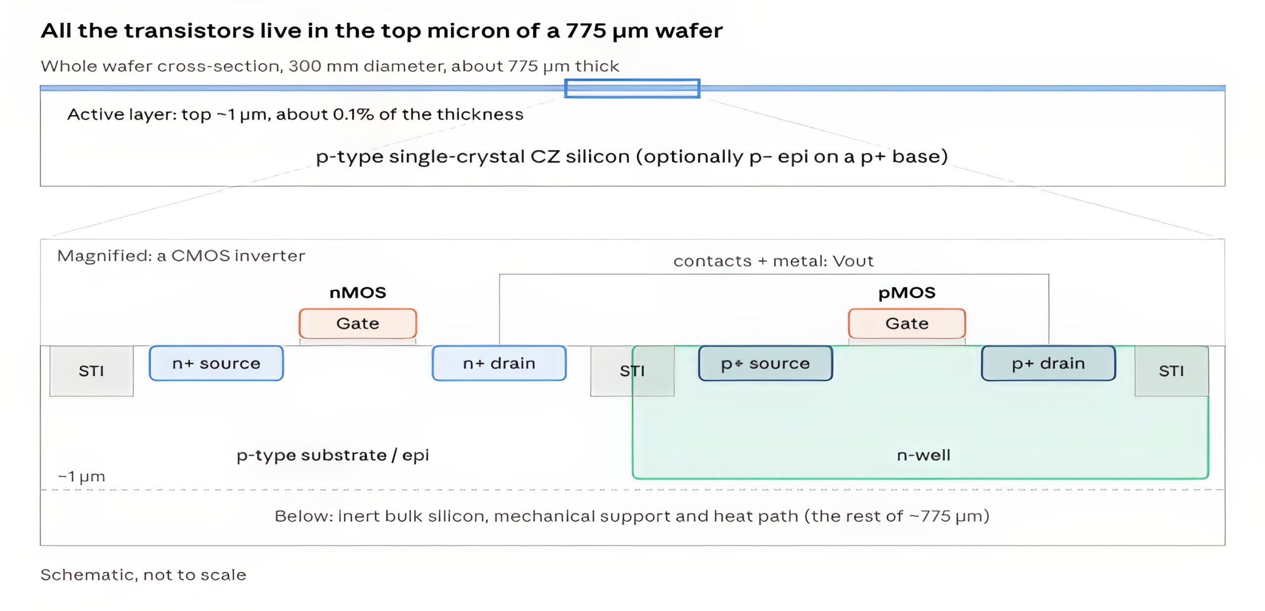
The nMOS sits directly in the p-type substrate, the pMOS in an n-well, separated by shallow trench isolation; everything below about 1 µm is passive silicon, yet it stays electrically connected to every device.
From sand to slice
- Quartzite is reduced to metallurgical-grade silicon, then refined (Siemens process) to electronic-grade polysilicon at 9N–11N purity.
- A Czochralski (CZ) puller dips a seed crystal into the melt and draws a single-crystal ingot, typically lightly p-doped with boron. Float-zone (FZ) growth gives lower oxygen content for power and detector devices.
- The ingot is ground, notched, sliced by wire saw, lapped, etched and chemically-mechanically polished to a mirror finish.
- Optionally, an epitaxial layer of a few microns is grown on top (p– on p+ epi), giving a cleaner, controlled-resistivity active layer over a heavily doped base.
How devices sit in it
In bulk CMOS, nMOS transistors are formed directly in the p-type substrate (or a p-well) and pMOS in an n-well. Source and drain are doped regions whose junctions face the substrate. Neighbouring devices are separated by LOCOS (field oxide) in older nodes and by shallow trench isolation (STI) from roughly 250 nm onward. The substrate is shared: every device is electrically coupled to it through junctions and the depletion region under its channel.
That shared, conductive body is both the strength of bulk silicon, I.E., cheap, mature, good heat path, and the root of its problems.
3. Drawbacks of bulk silicon
The conductive substrate couples every device to every other and to ground, and that coupling worsens as transistors shrink.
| Problem | Physical cause | Consequence |
| Junction capacitance | Large source/drain-to-substrate p-n junction areas | Slower switching, higher dynamic power (CV²f) |
| Latch-up | Parasitic p-n-p-n thyristor formed by wells and substrate | Supply short, chip destruction; needs guard rings, well taps |
| Short-channel effects | Gate loses control as drain field reaches through the deep channel region | Vt roll-off, DIBL, subthreshold leakage; requires heavy halo/pocket doping |
| Random dopant fluctuation | Few hundred dopant atoms in a scaled channel, placed randomly | Vt variability, poor SRAM low-voltage operation |
| Junction and substrate leakage | Reverse-biased junctions, GIDL, punch-through | Standby power, temperature sensitivity |
| Radiation sensitivity | Ion strikes generate charge collected over a deep volume | Single-event upsets and latch-up in space, avionics, automotive |
| Substrate noise and RF loss | Low-resistivity silicon conducts and couples signals | Crosstalk between digital and analog/RF blocks, lossy passives, poor switch linearity |
| Isolation | Junction or trench isolation only, never a true dielectric | High-voltage and mixed-signal integration costly |
By the late 1990s, at 180–130 nm, these effects were costing speed and power at each node. Designers compensated with process complexity (retrograde wells, halo implants, deep trenches), but the root cause remained the substrate under the channel. Removing it, or cutting it off with an insulator, was the obvious remedy.
4. The road to SOI
The idea is old: put a thin film of single-crystal silicon on an insulator, so each transistor is a dielectrically isolated island. Making that film cheaply and defect-free took about 30 years.
Early IC substrates
The isolation problem is as old as the germanium IC. Kilby’s (TI, 1958) and Noyce’s silicon planar (Fairchild, 1959) circuits led to commercial logic by 1961–62, built on 1–2 inch CZ wafers. Bipolar ICs used a p-type wafer with an n+ buried layer and an n-type epitaxial layer, with devices separated by p+ junction isolation. That isolation carried parasitic capacitance, leakage and parasitic transistors, the same drawbacks later seen in bulk CMOS. Dielectric isolation was used early for radiation-hard parts, through oxide-lined tubs in polysilicon (DI) and RCA’s silicon-on-sapphire in the mid-1960s, but at a cost only military and space programmes would pay. CMOS in the 1970s–80s simplified the substrate to lightly doped p-type wafers with wells, which is why it came to look like a commodity.
| Era | Method | How it works | Outcome |
| 1960s–80s | Silicon-on-sapphire (SOS) | Heteroepitaxial Si grown on sapphire | Radiation-hard military/space ICs; high defect density, expensive |
| 1970s–90s | Recrystallisation (ZMR, laser) | Melt and regrow poly-Si on oxide | Lab results only; crystal quality too poor |
| 1980s–2000s | SIMOX | High-dose oxygen implant + anneal forms buried oxide | Used by IBM and others; costly implants, defects, limited BOX control |
| 1980s–2000s | BESOI (bond and etch-back) | Bond two oxidised wafers, thin one by grinding/etch | Good for thick films; poor thickness uniformity for thin films |
| 1991 → | Smart Cut | Hydrogen implant defines a cleave plane; bond, split, polish, reuse donor | Became the industry standard |
Smart Cut
Smart Cut was invented by Michel Bruel at CEA-Leti in Grenoble in 1991, and Soitec was spun out in 1992 to industrialise it. The process:
- Oxidise a donor wafer; the oxide becomes the buried oxide (BOX).
- Implant hydrogen ions to a precise depth, creating a weakened plane.
- Bond the donor face-down onto a handle wafer.
- Anneal: the hydrogen platelets coalesce and the donor splits along the plane.
- Anneal and polish the transferred film to atomic-scale smoothness; reclaim the donor for reuse.
Film thickness is set by implant energy, so it can be controlled to within a few ångströms across 300 mm — the precondition for fully depleted devices. The same layer-transfer principle later carried over to other materials (piezoelectrics, SiC, III-V).
5. SOI in depth
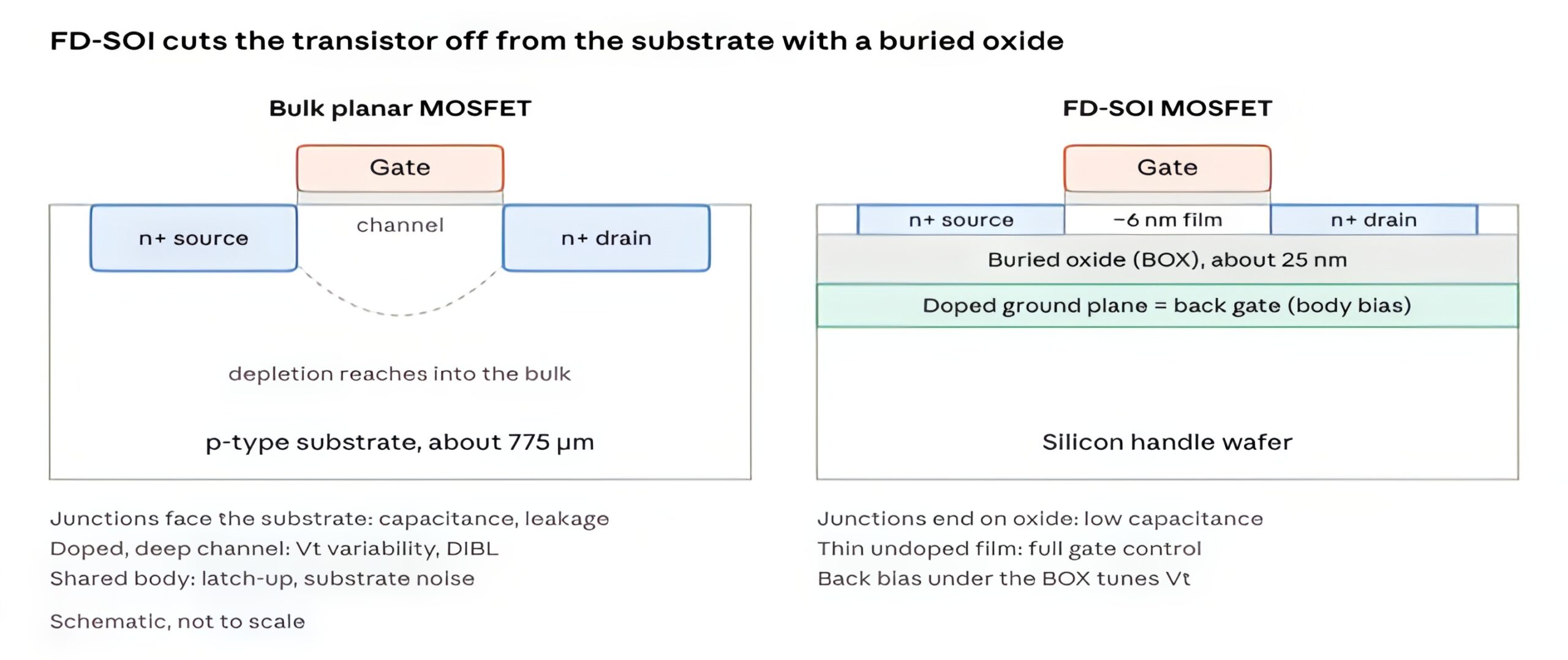
An SOI wafer is a three-layer stack: a thin top silicon film where devices live, a buried oxide (BOX) that isolates it, and a thick handle wafer for mechanical support. The thickness of film and BOX defines the flavour.
Partially vs fully depleted
- PD-SOI — top film thicker than the gate’s depletion depth (typically 50–100 nm). A neutral floating body remains under the channel. Used by IBM, AMD and Freescale in high-performance CPUs from 180 nm to 22 nm, and in game-console processors.
- FD-SOI — ultra-thin film (about 5–7 nm in the channel) over an ultra-thin BOX (about 20–25 nm). The film is fully depleted, so the channel needs little or no doping and the gate controls it completely. Shipped at 28 nm (ST, Samsung 28FDS), 22 nm (GF 22FDX) and 18 nm (ST/Samsung 18FDS), with GF 12FDX defined as the next step.
Back-biasing: the FD-SOI signature
Because the BOX is thin, the doped region under it acts as a second gate. Applying a voltage there shifts Vt by roughly 60–85 mV per volt. Forward body bias speeds the circuit when needed; reverse body bias cuts leakage in standby. The same silicon can be tuned after fabrication, per block and dynamically, which bulk FinFETs cannot do to any useful degree.
Application-specific SOI families
| Family | Key substrate feature | Main use | ||
| RF-SOI | High-resistivity handle plus trap-rich layer under the BOX | Antenna switches, LNAs, tuners in virtually every smartphone front-end | ||
| FD-SOI | Ultra-thin film and BOX | Low-power MCUs, IoT, automotive radar, mmWave, edge AI | ||
| PD-SOI | Thicker film | High-performance logic (legacy), some RF and analog | ||
| Power-SOI | Thick film and BOX | Smart power, gate drivers, automotive and industrial | ||
| Photonics-SOI | Controlled film and BOX for optical confinement | Silicon photonics waveguides, pluggable transceivers, co-packaged optics | ||
| Imager-SOI / MEMS-SOI | Tailored films | Near-infrared image sensors, MEMS structures | ||
Summary of Advantages
- Junction capacitance drops sharply (junctions end on the oxide), giving speed or power gains.
- No latch-up path; dense, simple isolation.
- Excellent electrostatic control in FD-SOI, without channel doping: lower DIBL, lower Vt variability, good low-voltage operation (down to about 0.4 V).
- Back-bias tunability for performance/leakage trade-offs.
- Charge collection volume reduced by orders of magnitude: strong soft-error and radiation tolerance.
- Low substrate loss and high linearity for RF; integration of RF, analog, digital and memory on one die.
- A planar process: fewer masks and simpler design than FinFET at comparable nodes.
6. Pitfalls of SOI
SOI’s costs are real, and they explain why it became a strong specialty platform rather than the mainstream logic substrate.
- Wafer cost. An SOI wafer costs several times a bulk prime wafer. Proponents argue the planar FD-SOI flow saves masks and steps versus FinFET, so the die cost is competitive; in practice the comparison depends on node and volume.
- Self-heating. The BOX conducts heat about 100 times worse than silicon. Transistors run hotter, which degrades mobility and reliability (electromigration, HCI) and complicates power devices and high-current I/O.
- Floating-body effects (PD-SOI). Charge stored in the undepleted body causes the kink effect, history-dependent delay and parasitic bipolar action. Body contacts fix it at an area cost. FD-SOI largely eliminates these.
- Film thickness control. Fully depleted devices need the film uniform to about ±0.5 nm across the wafer; any variation becomes Vt variation. Only a few suppliers can deliver this at volume.
- ESD and analog design. Thin films leave less silicon for ESD diodes and large analog devices; designers often open the BOX (hybrid bulk regions) for these.
- Limited scaling path. Below about 10 nm, film thickness would need to fall under 5 nm, where mobility and variability suffer. Leading-edge logic chose FinFET and now gate-all-around nanosheets instead.
- Ecosystem and supply concentration. Fewer foundries, PDKs and IP vendors than bulk; and one wafer supplier holds most of the thin-SOI market, a single-source risk customers weigh.
- Cyclic exposure. RF-SOI is tied to smartphone volumes. Soitec’s fiscal 2026 (Apr 2025–Mar 2026) shows this: Mobile Communications revenue fell 41% at constant currency on customer RF-SOI destocking (Soitec FY26 results).
7. Main players
The SOI value chain is concentrated: one dominant wafer maker, three Asian wafer licensees or competitors, and three FD-SOI foundries anchored in Europe.
Wafer suppliers
| Company | Base | Role in SOI | Status (2026) | |
| Soitec | Bernin, France | Smart Cut inventor-licensee; leader in RF-SOI, FD-SOI, Photonics-SOI, POI | FY26 revenue €592m (−34%); Photonics-SOI above $100m; CEO Laurent Rémont since Apr 2026 | |
| Shin-Etsu Handotai (SEH) | Japan | Largest silicon wafer maker; Smart Cut licensee, SOI producer | Second SOI source for major foundries | |
| SUMCO | Japan | Bulk wafer leader; SOI producer | Smaller SOI share | |
| GlobalWafers | Taiwan | Bulk and SOI, incl. ex-SunEdison SOI | Smaller SOI share | |
| Simgui (NSIG) | Shanghai, China | Soitec licensee for China; 200 mm and 300 mm SOI | Licence framework extended 10 years in Mar 2026 | |
Market-research firms commonly put Soitec’s share of the SOI wafer market well above half; figures vary by source and definition, so treat any single number as approximate.
Foundries and IDMs (FD-SOI)
| Company | Platforms | Fabs | Notes |
| GlobalFoundries | 22FDX, 12FDX, FDX Fusion; RF-SOI (8SW, 9SW) | Dresden, Malta, Singapore | Largest FD-SOI foundry; billions of chips shipped |
| STMicroelectronics | 28 nm and 18 nm FD-SOI with embedded PCM | Crolles, France | STM32V8 (18 nm, Cortex-M85, 800 MHz) and Stellar automotive MCUs |
| Samsung Foundry | 28FDS, 18FDS (co-developed with ST) | Giheung, Korea | eMRAM option; second source for ST |
| TowerSemi, UMC, others | RF-SOI | Various | Front-end module volume |
Research and ecosystem
CEA-Leti (Grenoble) is the technology origin and runs the FAMES pilot line for next-generation FD-SOI under the EU Chips Act. Design ecosystems include Synopsys, Cadence and Siemens EDA tool flows, plus IP vendors porting libraries with body-bias support. Major FD-SOI product users include NXP (i.MX), Sony (GPS), Lattice (FPGAs), automotive radar makers, and SpaceX via ST’s STM32V8 on Starlink.
8. What is next
The field is moving on two fronts: FD-SOI is heading below 10 nm for edge and physical AI, and the layer-transfer idea behind SOI is spreading to non-silicon materials.
FD-SOI goes single-digit. On 9 Oct 2026 GlobalFoundries announced FDX Fusion, a ground-up FD-SOI platform targeting 7 nm-class digital performance with more than twice the density of first-generation FDX, plus RF, analog, embedded NVM and in-memory compute. Demonstrator chips are due in early 2027, a first PDK in mid-2027, and production in Dresden in 2028 (Silicon Saxony / GF). CEA-Leti’s FAMES pilot line is developing 10 nm and 7 nm FD-SOI for Europe. FD-SOI’s pitch is not peak speed but performance per watt with RF and memory on one die — the profile of sensor fusion, robotics and radar.
Embedded memory on FD-SOI. ST’s phase-change memory at 18 nm and Samsung’s eMRAM replace embedded flash, which does not scale below 28 nm. This is what makes FD-SOI MCUs viable at advanced nodes.
Photonics-SOI and co-packaged optics. AI data centres need optical links at 800G–1.6T and beyond. Silicon photonics is built on SOI, and co-packaged optics (CPO) moves the optics next to the switch or accelerator. Soitec reports Photonics-SOI above $100m in FY26 and CPO qualification volumes in preparation for ramp-up — currently the fastest-growing SOI segment.
Engineered substrates beyond silicon.
- POI (piezoelectric-on-insulator) — thin lithium tantalate on silicon for high-performance SAW filters in 5G phones; multi-year supply agreement with Skyworks (Mar 2026).
- SmartSiC — a thin monocrystalline SiC layer bonded on a low-cost poly-SiC handle, aiming to cut SiC power-device substrate cost; slowed by the EV market (Soitec impaired €41m of SmartSiC assets in FY26).
- GaN-on-SOI and RF-GaN — for power and mmWave/6G front-ends.
- SOI for quantum and sensors — FD-SOI back-gating is used to control spin qubits at cryogenic temperatures (CEA, Quobly).
Substrate as a 3D building block. Layer transfer, wafer bonding and backside processing — the core Smart Cut skills — are now central to 3D integration, backside power delivery and hybrid bonding in leading-edge logic. Even where the final chip is not SOI, the substrate-engineering know-how is.
Open questions
- Will FDX Fusion and 10 nm FD-SOI find enough volume customers to justify the investment against 3 nm-class GAA for edge AI?
- When will RF-SOI inventories normalise, and how much will 5G/6G front-ends grow SOI content per phone?
- Can China’s SOI supply (Simgui and others) shift market share as local foundries adopt FD-SOI?
9. Summary and glossary
Bulk silicon is cheap and thermally friendly, but its conductive body couples devices to each other and limits leakage, variability, RF and radiation performance. SOI cuts the transistor off from that body with a buried oxide; Smart Cut made it manufacturable. Leading-edge logic chose FinFET and GAA instead, but SOI owns smartphone RF front-ends, is growing in silicon photonics, and FD-SOI is the reference low-power platform for MCUs, radar and edge AI — now with a sub-10 nm roadmap.
| Term | Meaning |
| BOX | Buried oxide; the insulating SiO2 layer in SOI |
| CZ / FZ | Czochralski / float-zone crystal growth |
| DIBL | Drain-induced barrier lowering; a short-channel effect |
| FBB / RBB | Forward / reverse body bias via the FD-SOI back gate |
| FD-SOI / PD-SOI | Fully / partially depleted SOI |
| GAA | Gate-all-around (nanosheet) transistor |
| POI | Piezoelectric-on-insulator substrate |
| Smart Cut | Hydrogen-implant layer-transfer process (CEA-Leti, 1991) |
| STI | Shallow trench isolation |
| Trap-rich layer | Polysilicon under the BOX in RF-SOI that suppresses parasitic surface conduction |
Sources
- Soitec — Fiscal 2026 full-year results (27 May 2026)
- Silicon Saxony — GlobalFoundries FDX Fusion roadmap (9 Oct 2026)
- Mobile World Live — ST launches 18 nm STM32V8
- CEA-Leti — FD-SOI next generation 10–7 nm
Further reading
- M. Sze, Physics of Semiconductor Devices, for the bulk MOSFET and CMOS
- -P. Colinge, Silicon-on-Insulator Technology: Materials to VLSI, for SOI and FD-SOI
[1] FD=Fully Depleted. The top silicon film is about 5–7 nm so that the gate’s depletion region spans its whole thickness, leaving no neutral, undepleted silicon under the channel. That is what gives FD-SOI tight gate control without channel doping and removes the floating-body effects of PD-SOI (Partially Depleted), where the film is thicker and a neutral body remains
Share this post via:


Comments
There are no comments yet.
You must register or log in to view/post comments.