By Philippe Flatresse, Bich-Yen Nguyen, Rainer Lutz of SOITEC
I. Introduction
Automotive radar is a key enabler for the development of advanced driver assistance systems (ADAS) and autonomous vehicles. The use of radar allows vehicles to sense their environment and make decisions based on that information, enhancing safety and driving performance. Automotive Radars are considered very robust against disturbing atmospheric and environmental factors being able to instantaneously measure distance, angle and velocity and produce detailed images of the surroundings.
Initially developed for high class vehicles, the radar has gained considerable momentum over the past 2 decades. The first mass-produced 77Ghz radar was implemented in a Mercedes-Benz S-Class in 1998. Eight years later it was followed by a more advanced system combining 77Ghz long range radar (LRR) with two 24GHz short range radar (SRR) sensors to fit the urban traffic [1]. In 2011, the democratization of automotive radar has clearly begun with the adoption of standard series product in middle class vehicles.
Ten years later, the worldwide automotive radar market is primarily driven by rising demand for advanced driver assistance systems and further accelerated by the requirement for active safety systems mandated by government laws or new car assessment program such as NCAP. The global automotive radar market has grown in response to the increased use of radar equipment per vehicle. Several new car models have announced that they will have up to 10 radar sensors per vehicle starting 2025, which will enable the creation of a radar-based 360° surround view necessary for advanced driver assistance and semi-autonomous operation. As a result, the automotive industry is currently experiencing a high demand for high-precision, multi-functional radar systems, which has led to increased research and development activities in the field of automotive radar systems.
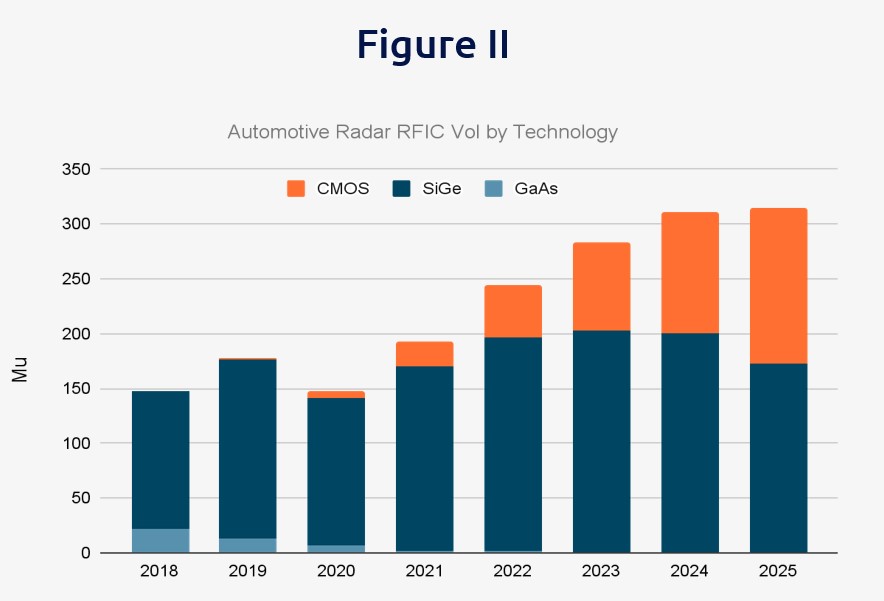
To meet the demands of the next generation of radar systems, the move to advanced CMOS technology is considered to be a necessary transition. Adopting CMOS technology allows for a significant increase in the density of integration, making it possible to create a radar transceiver that is entirely integrated onto a single chip, known as a radar system on chip (SoC). This type of design typically includes the millimeter wave frontend, analog baseband, and digital processing all on the same chip. It may also include MCUs, DSPs, memory, and machine learning engines, allowing the radar to operate independently with very few external components, thus reducing the overall BOM cost. The main nodes of choices today are 40/45nm, 28nm, and 22nm. Some are even going for 16nm.
One of the most promising silicon technologies for automotive radar already identified by several module makers is fully depleted silicon-on-insulator (FD-SOI) [2, 3]. FD-SOI technology enables the integration of high-frequency radar components on a single chip. The technology can not only improve the performance of the radar system but it also allows for low-power operation, which is critical for automotive applications where power efficiency is a concern.
II. Automotive Radar trends
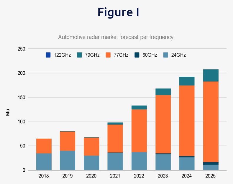
The use of radar technology in vehicles is expected to continue growing, driven by both an increase in the number of cars adopting radar and by the amount of radar content per vehicle. These trends are driven by the growing adoption of advanced driver assistance systems (ADAS) and will be further sustained and strengthened in the long-term by the development of highly automated or autonomous driving. According to several market reports [4,5], the global automotive radar market size accounted for USD 6 Billion in 2021 and is estimated to achieve a market size of USD 22 Billion by 2030 growing at a CAGR of 20% from 2022 to 2030. In other words, the sales of automotive radar (SRR, MRR, and LRR) for level 2 and above are projected to experience significant growth in the coming years from 100 million units in 2021 to 400 million in 2030, meaning 4X increase in less than one decade. It is worth mentioning that 50% of the automotive radar will be manufactured in CMOS technologies by 2025.
The technology of automotive radar sensors has evolved over the years since its first introduction in 2000. Previously, automotive radars were mainly used in the 24 GHz frequency band for short-range detection and in the 76-77 GHz range for longer range or more complex applications. It is important to notice that the European Telecommunications Standards Institute (ETSI) and the Federal Communications Commission (FCC) have allocated a specific frequency band between 76 GHz and 81 GHz for automotive radar applications. However, due to difficulties in designing efficient and cost-effective integrated circuits at such high frequencies, a temporary frequency band around 24 GHz was also made available to manufacturers to develop 77 GHz radar transceivers. With advancements in technology, 77 GHz radar products are now well-developed, and the temporary 24 GHz frequency band is no longer available since 2022. Nowadays, the trend has shifted towards using the 76-81 GHz frequency band for the development of new sensors. While research into even higher frequency bands above 100 GHz is ongoing, the integration of these technologies into vehicles and the challenges related to semiconductor technology performance are still being studied.
III. Automotive Radar challenges
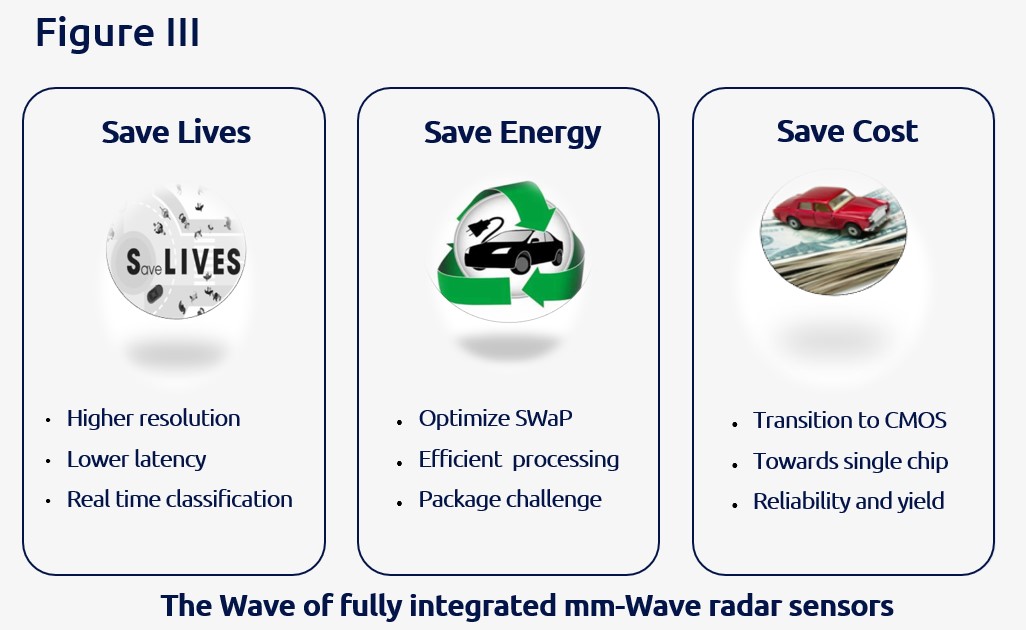
Automotive radar technology plays is a crucial component in the development of advanced driver assistance systems (ADAS) and autonomous vehicles. However, the development and implementation of automotive radar systems comes with several challenges, including the need to save lives, energy, and costs (Fig.3).
Save Lives: Automotive radar technology needs improve the safety of vehicles by providing advanced warning of potential hazards on the road. To save lives, automotive radar must have high resolution to accurately detect and identify objects, low latency to provide timely warnings to the driver, and real-time classification capabilities to distinguish between different types of objects, dealing with the environmental conditions (like fog, rain, dust and other factors) that can affect the accuracy of the radar. These features allow the radar to detect and track objects such as other vehicles, pedestrians, and animals, and provide the driver with the information they need to make safe decisions on the road. Improving the resolution, latency, and classification capabilities of automotive radar technology can help to reduce accidents and save lives.
Save Energy: Automotive radar technology can also play a role in saving energy by optimizing the size, weight, and power (SWaP) of the system. This can be achieved by using efficient processing techniques and reducing the size and weight of the radar’s package. Optimizing SWaP is particularly important in electric vehicles (EVs) and hybrid electric vehicles (HEVs) where energy storage is limited. Reducing the size and weight of the radar system can also help to reduce the overall vehicle weight and improve fuel efficiency.
Save Costs: Transitioning to complementary CMOS technology is one way to reduce the cost of automotive radar systems. CMOS is a widely used manufacturing process for integrated circuits that allows for the integration of multiple functions onto a single chip. Single-chip solutions can further reduce costs by integrating all the necessary components and functions of the radar system onto a single chip. This can help to reduce the size and weight of the radar system, as well as simplify the manufacturing process. Reliability and yield are also important factors to consider when mass-producing automotive radar systems.
The success of advanced driver assistance systems (ADAS) and autonomous vehicles depends on the ability to address the challenges related to safety, energy efficiency and cost-effectiveness. A critical aspect in this regard is the choice of silicon technology, with a clear shift nowadays towards the use of CMOS technology. The technology that will dominate this field will be the one that can provide high resolution, low latency, and accurate classification, reduce energy consumption, simplify the manufacturing process and reduce costs by offering fully integrated radar systems.
IV. Automotive radar key metrics
The radar sensor is tasked with identifying and spatially locating mass-based obstacles. These can include other vehicles, bicyclists, pedestrians, animals, and even fixed obstacles. The key metrics when analyzing the performance of a radar sensor is how far it can detect object (range), how reliably it can resolve objects (range resolution), how much it can resolve velocity of objects (velocity resolution) and how accurate it can determine object position and trajectory (angle resolution). The table below gives the technical requirements of automotive radar sensor.
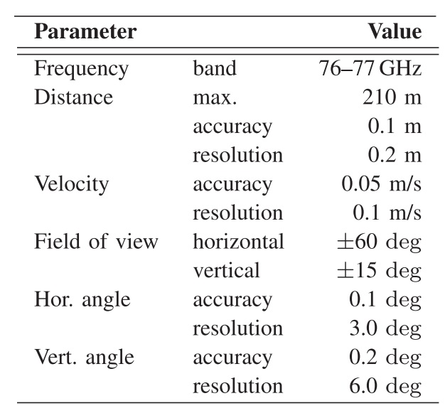
Let’s have a look now to the requirements to fulfill the key metrics of automotive radars:
- Range: One of the range requirements is a high power transmitter, as it allows the radar to detect objects at a greater distance. A high sampling rate is also necessary to accurately determine the location and velocity of objects. Solutions to achieve these requirements include the stacking of multiple devices to increase the power output, and the use of low power and high linear ADC to efficiently process the radar signals.
- Range and velocity resolution: Resolution refers to the ability of the radar to differentiate between objects that are close together. To improve resolution, one approach is to move to higher frequency bands, as the wavelength of the radar signal decreases with increasing frequency, allowing for finer resolution. Solutions to achieve this include using higher Ft/Fmax technologies in the radar signal. This allows for higher frequency components to be used in the signal, which can result in improved resolution.
- Angle resolution: To improve angle resolution, one of the requirements is to limit thermal issues, as high temperatures can affect the performance of the radar’s electronic components. One solution to this is to improve the power amplifier (PA) and digital efficiency of the radar system. By increasing the efficiency of the PA and decreasing the digital power, less heat is generated, which can help to reduce thermal issues.
This section highlights the importance of having top-notch silicon technology with cutting-edge analog and millimeter wave RF capabilities in order to tackle the technological challenges posed by future automotive radars. Such technology must be able to handle a large amount of data while maintaining low power consumption.
V. FD-SOI technology, do more with less energy
The current major technology shift in the radar segment is the adoption of CMOS technologies. Current CMOS technologies available for automotive such as 40nm, 28nm, 22nm, 16nm provide a high level of integration for digital circuits and exhibit very good performance in RF applications. Using CMOS technology to design automotive radar systems allows for a number of advantages over traditional analog radar transceivers. One of the main benefits is that CMOS allows for the integration of multiple components, such as the radar transceiver, signal processing circuits and control logic, into a single chip. This improves the resolution and density of the radar system, allowing for more accurate and reliable detection of objects. Additionally, CMOS technology is also generally less expensive than traditional analog radar transceivers, which help to lower the overall cost of the radar system. By having the radar system on a single chip, the SoC can be more compact and power efficient, which is important in automotive applications where space and power consumption are both important.
One way to evaluate the suitability of CMOS technology for automotive radar operating at 77 GHz is to look at the speed of the transistors. The table 2 below compares the fT and fmax of various state-of-the-art CMOS technologies. These values give an indication of how fast the transistors can operate and therefore how well they can handle high frequency signals, making it a good indicator of the feasibility of using CMOS technology in automotive radar. Today, the transit frequencies achieved allow CMOS technologies to penetrate the radar automotive market traditionally dominated by BiCMOS processes representing more than 2/3 of the overall radar market as of today. As shown in Table 1, among CMOS processes currently used for radars, the 22nm FD-SOI technology clearly outperforms both finfet and bulk technologies and is on par with the state of art SiGe technologies. This technology is seen by several radar chip makers, such as Bosh or Arbe, as state of the art CMOS technology for radars with the ability to offer transistors of ft > 350 GhZ ad Fmax > 390 GhZ and several additional unique benefits that are described in the next sections.

a. Unique features of FD-SOI technology
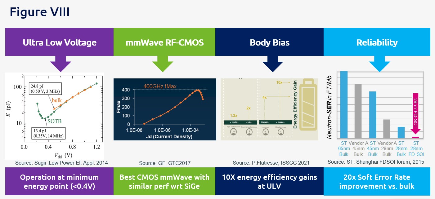
FD-SOI is a well-known technology in the field of semiconductors allowing for improved performance and lower power consumption compared to traditional bulk silicon technology. FD-SOI technology allows for more flexibility in the design and manufacturing process, making it a popular choice for a wide range of applications, including automotive radar systems. FD-SOI transistors offer several unique features, such as the ability to operate at low voltage, to cancel PVTA variations, to be quasi-insensitive to radiation and to exhibit a very high intrinsic transistor speed, which make it an ideal choice over other RF-CMOS technology alternatives (Figure 8).
i. FD-SOI and Ultra Low Voltage
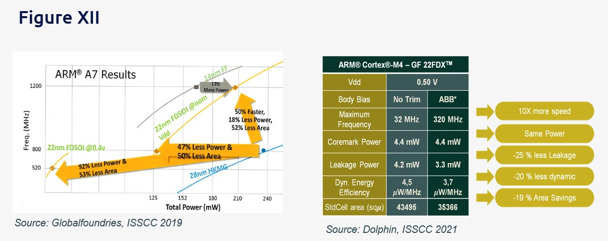
Thanks to its intrinsic low-variability characteristics and body bias techniques, FD-SOI is able to operate at very low supply voltages down to 0.4V or below, making it an ideal technology for applications where power consumption is a critical concern. Lowering the supply voltage reduces the dynamic power consumption offering a unique advantage over other technologies, as it allows for more efficient power usage in applications where power is more of a challenge than performance.
ii. FD-SOI and Soft Error Rate
FD-SOI is known for its high resistance to high-energy particles, which can cause soft errors in electronic devices. This is because in FD-SOI, the active device region is separated from the substrate by a thin insulating layer called the Box. The buried oxide layer reduces the susceptibility of the device to charges generated in the substrate, making it less likely to experience soft errors. This feature makes FD-SOI a suitable technology for safety-critical applications such as advanced driver assistance systems (ADAS) and autonomous driving systems (AD).
iii. FD-SOI and Body Biasing
Another key advantage of FD-SOI is body biasing. The body biasing allows taking control of the threshold voltage of the device post-fabrication. Body bias is a very powerful knob in automotive applications and has been widely deployed for PVTA compensation in many consumer and automotive products already. By implementing body biasing in a product, significant reductions in process, voltage, temperature and aging variation can be attained, simplifying the task of product engineers to ensure product specifications at a 1-ppm [10].
Body Biasing is a must have in the next radar generation as a key technique to improve the digital and the analog as well as reliability.
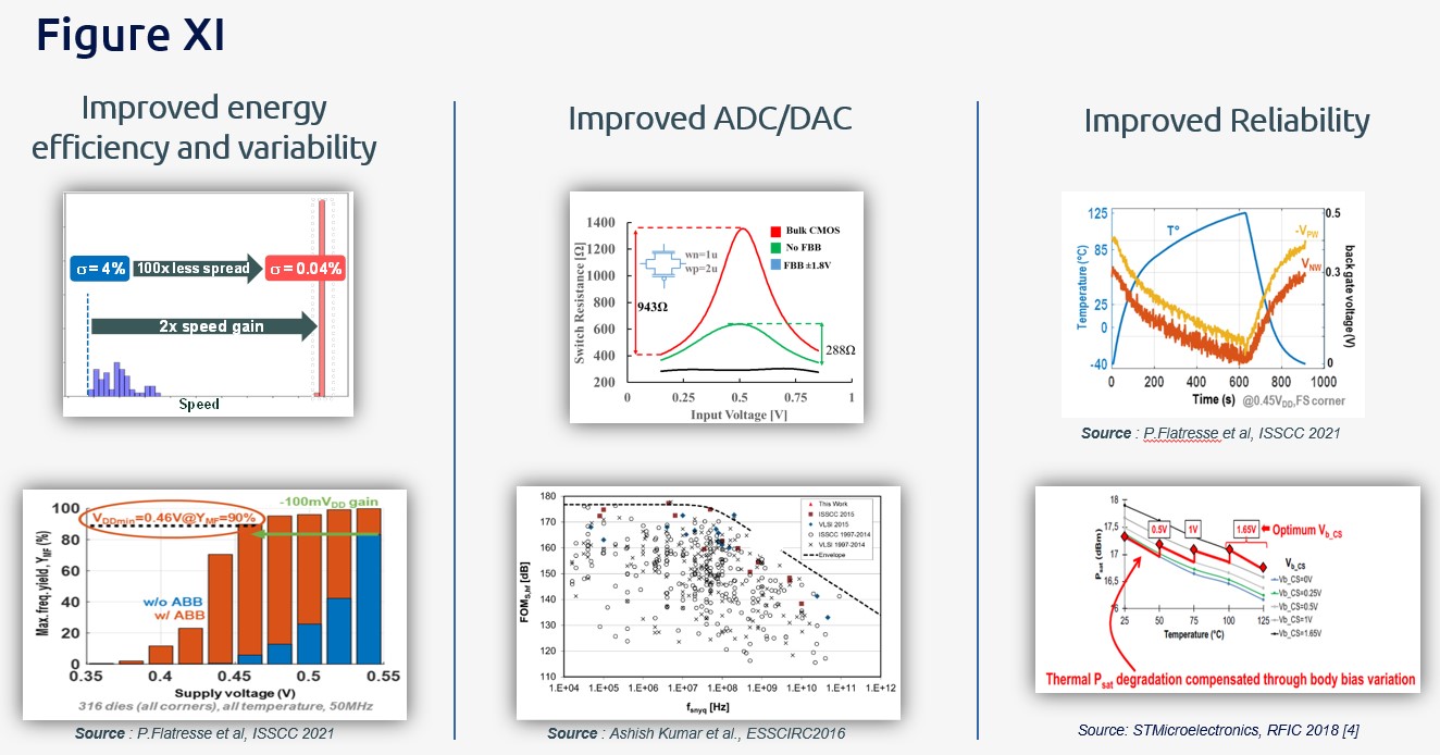
On the digital side, new adaptive body biasing techniques (ABB) have been recently developed allowing the application design to maintain a targeted operating frequency over a wide range of operating conditions such as temperature, manufacturing variability and supply voltage [12]. The architecture enables to reduce energy consumption of processors in 22nm FD-SOI technology by up to 30% and increase the operating frequency up to 450% compared to a technique in which body biased technique is not used [20].
In analog circuits, body bias has several benefits in analog circuits. One of the most significant benefits is improved accuracy, which can be achieved by fine-tuning the performance of the circuit. Additionally, body bias can also reduce power consumption by controlling the operating point and reducing leakage currents. Furthermore, body bias increases the voltage headroom of the circuit, allowing it to operate over a wider range of supply voltages. Body bias also improves the noise immunity of the circuit by reducing the threshold voltage and increasing the drain current. Lastly, body bias can be used to optimize the performance of the circuit for specific applications, such as low-power, high-speed, or high-linearity. These benefits make body bias a valuable knob for trading-off between different performances characteristics such as power consumption, speed, and linearity of analog circuits. [17]
On the reliability side, by controlling the operating point of transistors, body bias can reduce stress on the devices, leading to improved reliability. Additionally, body bias can compensate for temperature-related changes in the threshold voltage, making the circuit more temperature stable. Body bias can also reduce the threshold voltage and increase the drain current, improving the immunity to single event effects such as cosmic rays and alpha particles. Dynamic reliability drift compensation is also a promising area of research that holds the potential to produce fully resilient automotive systems [11]. Furthermore, body bias can reduce the degradation of the threshold voltage over time, leading to improved aging performance. Finally, body bias can compensate for variations in the threshold voltage due to manufacturing processes, making the circuit more robust. These benefits make body bias a valuable tool for improving the reliability of analog circuits.
iv. FD-SOI and Analog/RF
As speed, noise, power, leakage, and variability targets are becoming more and more difficult to meet, FD-SOI technology offers a solution by providing improved matching, gain, and parasitics in transistors, thus simplifying the design of analog and RF blocks. Combining as many analog/RF functions as possible into a single RF-CMOS silicon platform is becoming more vital for cost and power efficiency, but RF-CMOS platforms struggle with increasing frequency, particularly in the mmWave spectrum. FinFETs have even more limitations architecture, so SiGe-Bipolar platforms are often used in this frequency range. FD-SOI, being a planar technology, does not have the limitations of 3D devices, with Ft/Fmax in the range of 350 GHz to 410 GHz reported, enabling full utilization of the mmWave spectrum, making FD-SOI RF-CMOS platforms a promising option for various applications such as automotive radars.
v. FD-SOI and performance booster
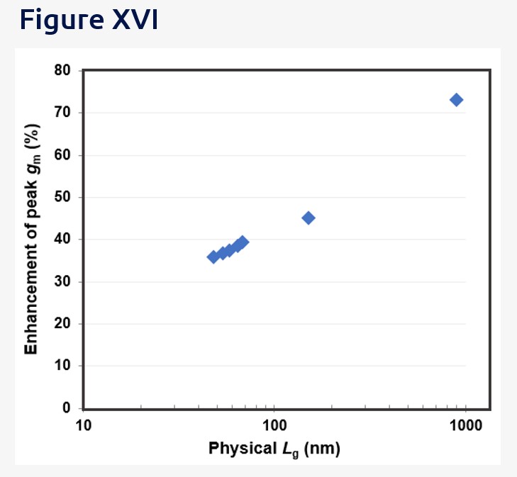
Smartcut technique has been used to transfer the biaxial strain silicon film that grown pseudo-morphically on the fully relaxed SiGe buffer layer on Si bulk as a donor wafer to form the unique strain Si on Insulator (SSOI) wafer. The SSOI technology is a nature extension of the SOI technology, combining the advantages of the FD-SOI and the carrier mobility enhancement of the tension strain silicon. The biaxial tension strain Si and compression SiGe which can be formed by partially relaxed the tension strain and then locally Ge condensation [18] to boost the performance of n-channel and p-channel transistors, respectively [19] for boosting performance of logic and RF as shown in Figures 15. The saturation current (Ion) of the n-channel FD-SOI device gains 28% with 20% tension strain Si channel (Fig. 15.a) and 16% Ion gain for 35% c-SiGe formed by Ge condensation without relaxed the tension strain by Ar or Si implant prior to Ge condensation (Fig. 15.b). Using partial tension strain relaxation prior to form cSiGe channel will gain higher performance to great than 20% with 25% cSiGe. Figures 15.c&d show further performance gain with segment the width of channel (W) into multi narrow W to convert the biaxial strain into uniaxial strain which can further improves the performance up to 50% gain for the same strain level. Figure 16 shows the transconductor gain as a function of the gate length, the performance of longer gate length is less limited by parasitic resistance thus its performance gains closer to the mobility gain. The geometry impacts by the strain channel material on performance gain should be considered to maximize the benefits of the strain materials.
Strained Si on silicon-on-insulator (SSOI) is a natural extension of SOI, combining the advantages of SOI and the carrier mobility enhancement of tensile-strained Si for high-performance low-power applications [4].
a. FD-SOI benefits for radar system-on-chips
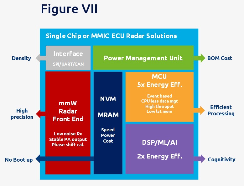
A system-on-chip (SoC) that integrates the analog front-end and digital signal processing is a logical choice for the next generation of radar technology, as it allows for the efficient and extensive monitoring of multiple parameters and real-time evaluation during sensor operation, which is mandatory for being eligible for safety-critical applications. As shown in the block diagram in Figure 7, a fully integrated mmWave radar includes transmit (TX) and receive (RX) radio frequency (RF) components; analog components such as clocking; and digital components such as analog-to-digital converters (ADCs), microcontrollers (MCUs) and digital signal processors (DSPs). Traditionally, the radar systems were implemented with discrete components, which increased power consumption and overall system cost.
FD-SOI appears as an ideal technology and a natural evolution for automotive radars. FD-SOI technology combines the high mobility of undoped channel, smallest total capacitance for same design rule, low power digital capabilities with the option for Si-base mobility booster, these greatly enhanced performances for both digital and RF/mmWave functions, providing an ideal platform to develop fully integrated radar device.
i. Unrivalled energy efficiency
Power efficiency is a critical consideration for every automotive sensor application. Whether powered by fossil fuel or electricity or a combination of the two, the energy consumption and the thermal management constraints compound the power efficiency challenge of the vehicles. The radar sensor processing requires the utmost attention to performance-per-watt metrics. In this domain, FD-SOI exhibits a clear advantage compared to competing approaches. FD-SOI offers significant energy efficiency improvements for MCUs and DSPs over other CMOS technologies. At a given technology node, FD-SOI can consume up to 40% less power or operate 30% faster than equivalent transistors. It allows boosting the performance at constant power level, making it ideal for low power or thermally constraint applications. Additionally, sensors with a 20% smaller form factor can be designed in FD-SOI leading to reduced costs for the overall system and package. Overall, FD-SOI technology is a cost-effective and power-efficient solution for sensor applications, making it well suited for low-power mm-wave radar systems. The benefits can lead to improved imaging radar resolution, more features in the same footprint and reduced BoM cost.
ii. State of the Art CMOS Power Amplifier
Power amplifiers (PAs) play a critical role in automotive radar systems, as they are responsible for amplifying the weak radar signals that are transmitted and received by the radar antenna. When designing a power amplifier (PA) for radar systems, several key factors must be taken into consideration to ensure optimal performance.
- High efficiency in saturation: The PA should be able to operate in saturation mode, which is commonly used in Frequency Modulated Continuous Wave (FMCW) radar systems, to achieve high efficiency while still providing a strong radar signal. For Pulse Modulated Continuous Wave (PMCW) radar systems, the PA should be able to achieve high efficiency even when operating with some back off, as linearity is required in the PA to ensure accurate radar measurements.
- High output power: The PA must be able to provide a high output power to ensure a strong radar signal and a long detection range.
- Stability of performance over temperature: The PA should be able to maintain stable performance over a wide range of temperatures, as automotive radar systems are subjected to harsh environments.
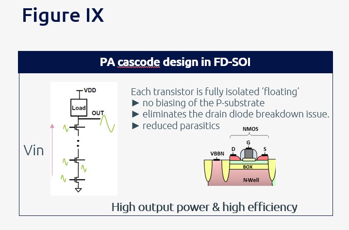
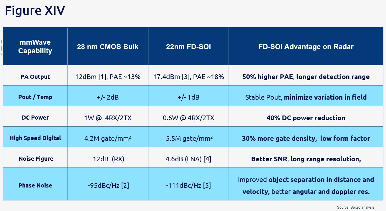
FD-SOI technology brings several advantages when designing power amplifier (PA) for radar systems. One of the most significant benefits of FD-SOI technology is its high efficiency. Intrinsically, the PA in FD-SOI provides high output power due to the high breakdown voltage of the fully depleted transistors. In CMOS technologies, the design of the PA is based a cascade architecture to increase power handling capability. The cascode stage acts as a buffer and provides additional gain, which improves the overall performance of the PA. One of the main limitations of using cascode architecture in bulk or Finfet is that it sees high drain-to-substrate voltage due to the biasing of the P-substrate. In FD-SOI, each transistor is fully isolated, or “floating,” which means that there is no direct contact between the substrate and the active devices as shown in figure 9. This eliminates the need for substrate biasing, which can reduce the drain-to-substrate voltage and improve the overall performance of the PA. The stacking in FD-SOI can reach up to 50% higher PAE compared to other technologies, as this allows for the input power to be distributed among multiple devices, reducing the power loss due to heat. In the context of radar, higher performance can be achieved for both long-range Radar (LRR) and short range radar (SRR) using FD-SOI. Another important factor to consider is the stability of performance over temperature. When assisted with back gate bias, the high thermal stability of FD-SOI technology can easily be maintained enabling a tight output power control over a wide range of temperatures [13]. +/- 1dB variation over 145 degree temperature change is presented in [14], a crucial result for automotive radar systems that are subjected to harsh environments. Finally, in terms of reliability, FD-SOI PAs exhibit also better reliability figures due to the absence of lateral bipolar and higher breakdown voltage allowing a larger swing. Overall, FD-SOI technology provide a optimum solution for automotive radar power amplifiers, providing high efficiency, high linearity, high output power, high reliability, and stability over a wide range of temperatures.
iii. Low Power ADCs
Automotive radar systems prioritize performance at mmWave frequencies over the specific requirements of the ADC (Analog-to-Digital Converter). However, the ADC still plays a important role in the overall system performance. The ADC should have low power consumption, particularly for high sampling rates, such as in Pulse-Modulated Continuous-Wave (PMCW) radar systems. Additionally, the ADC should have high linearity to accurately convert the analog signal to digital, and should be able to compensate for variations in process, voltage, and temperature (PVT). These requirements are important to ensure that the radar system operates correctly and accurately in real-world automotive environments.
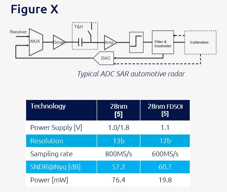
The automotive radar ADC in FD-SOI (Fully-Depleted Silicon-on-Insulator) technology has several advantages for low power consumption. The smaller switches in FD-SOI have lower Ron (resistance) and lower parasitics, which results in higher SNDR (Signal-to-Noise-and-Distortion Ratio) and better switch linearity. Additionally, the FD-SOI technology allows for the use of lower power supply voltages, which further reduces power consumption.
In [15], comparing the ADC performance of 28nm BULK and 28nm FDSOI technology, it can be seen that the FDSOI technology has a lower power supply voltage of 1.1V as opposed to 1.0/1.8V, which leads to a significant reduction in power consumption from 76.4mW down to 19.8mW. The FDSOI technology also has a higher SNDR of 60.7 dB at a Nyquist frequency, as compared to 57.2 dB for the BULK technology. Overall, the use of FDSOI technology in automotive radar ADC results in lower power consumption and improved performance.
b. FD-SOI ideally positioned for the radar applications
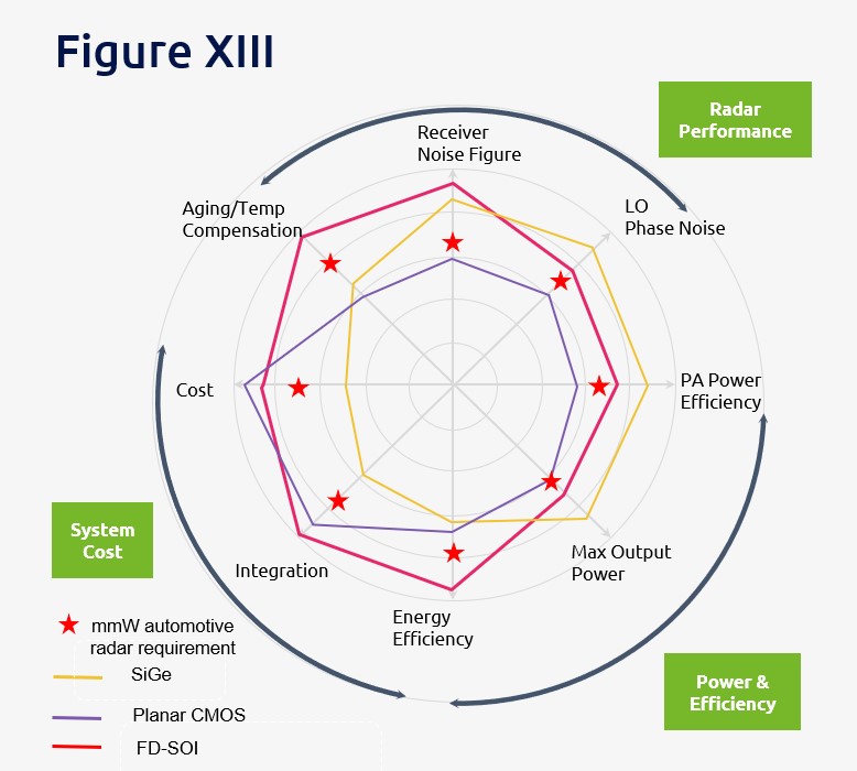
FD-SOI technology is ideally positioned for radar applications due to its advantages in system cost, power efficiency, and radar performance. Compared to alternatives technologies such as SiGe or planar CMOS technologies as shown in figure 13, FD-SOI offers higher integration capability, better receiver noise figure and also built-in aging and temperature compensation solutions that can be easily implemented using body bias techniques. On top, the technology also exceeds the mmW automotive radar requirements in terms of output power and power amplifier efficiency. In few words, FD-SOI is well-suited for cost-sensitive automotive radar applications requiring significant processing and RF mmW capabilities at lower power consumption.
VI. FD-SOI and High Resistivity substrate
The CMOS mmWave era opens up the door to revolutionary applications in the fields of ADAS and AD. FD-SOI technology is entering those filed as a versatile and flexible solution, seen as a digital technology with state of the art RF/mmWave capabilities. The technology provides significant benefits in terms of resolution, velocity, power consumption and cost requested by the radar market.
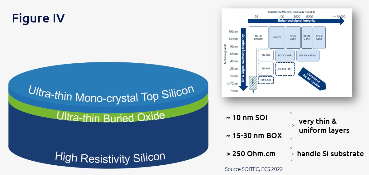
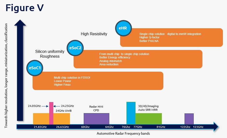
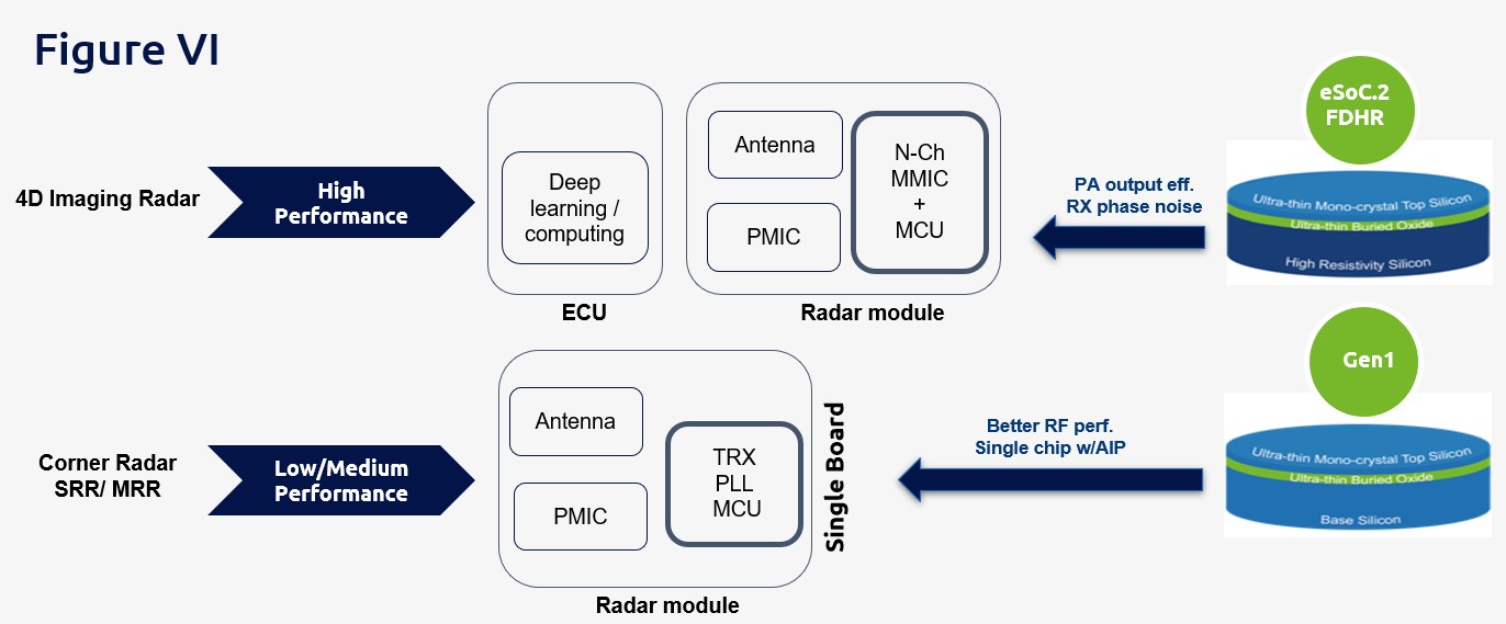
A clear trend is the increasing differentiation of standard cost-effective sensors for driver assistance applications and high-performance sensors for autonomous driving. Future radar applications, such as 4D imaging, impose new levels of performance for both RF and logic devices. To fulfill all the requirements, additional improvements at substrate level are mandatory. The high resistivity option is seen as a new leveler to further enhanced performance of RF devices (Fig.4). High resistivity SOI substrate has been widely adopted in the smartphone market, being currently present in 100% of them. It is clearly a valuable option for next generation automotive radar, FD+HR yields best-in-class passive-loss, increasing efficiency and reducing floorplanning. The high resistivity option in FD-SOI is seen as a major booster to reach ultimate mmW performance, enabling a higher level of SoC integration with unrivalled RF-mmW characteristics. It is important to highlight that SOITEC has designed a new substrate that avoids device integration changes of existing 28nm, 22nm and future 18nm, 12/10nm technology nodes (Fig.5) [16].
VII. Conclusion
In conclusion, FD-SOI is playing a crucial role in shaping the future of automotive radar. Its intrinsic key features make it a valuable technology for the automotive radar industry. FD-SOI enables the development of single chip high performance and cost-effective radars, making it a crucial enabler in vehicle safety and autonomous driving. Its ability to increase computing power while maintaining energy efficiency and intelligence opens the door to disruptive innovations and SWaP optimizations FD-SOI technology can definitively help drive a safe transition to CMOS technologies in the automotive radar industry.
VIII. Graphs
![White paper Figure 15 Figure 15: Ion vesus Ioff of (a) SOI vs. sSOI for n-FET, (b) SOI vs cSiGeOI p-FET, (c)35% cSiGeOI p-FET with different W. (d) 35% cSiGeOI p-FET Ion and µ gain versus W [Ref.a]](https://semiwiki.com/wp-content/uploads/2023/10/White-paper-Figure-15.jpg)
VIII. References
- [1] Holger H. Meinel and Juergen Dickman, “Automotive Radar: From its origin to future directions”, Microwave Journal, 2013
- [2] ee-News Automotive, “Arbe moves to production of 4D radar chipset”, Business News, 2022
- [3] David Manners, “Bosch to use FD-SOI for automotive radar SoCs”, Electronics Weekly, 2021
- [XX] K. Ramasubramanian, “Moving from legacy 24 GHz to state-of-the-art 77 GHz radar.” Texas Instrument, 2017.
- [4] Acumen Research and Consulting , “Automotive Radar Market Report and Region Forecast, 2022 – 2030” , 2023
- [5] Yole Development , “Status of the Radar Industry: Players, Applications and Technology Trends” , Market and Technology Report, 2020
- [6] Christian Waldschmidt et al., “Automotive Radar—From First Efforts to Future Systems” , IEEE Journal of Microwave, 2021
- [7] Philipp Ritter, “Toward a fully integrated automotive radar system-on-chip in 22 nm FD-SOI CMOS” , International Journal of Microwave and Wireless Technologies, 2021
- [8] Nobuyuki Sugii, “Ultralow-Power SOTB CMOS Technology Operating Down to 0.4 V”, Journal of Low Power Electronics and Applications
- [9] Nobuyuki Sugii, “Ultralow-Power SOTB CMOS Technology Operating Down to 0.4 V”, Journal of Low Power Electronics and Applications
- [10] P. Flatresse, “Process and design solutions for exploiting FD-SOI technology towards energy efficient SOCs”, International Symposium on Low Power Electronics and Design (ISLPED), 2014.
- [11] P. Flatresse, “RBB & FBB in FD-SOI” SOI Forum, Shangaï, 2017
- [12] A. Bonzo et al. “A 0.021 mm² PVT-Aware Digital-Flow-Compatible Adaptive Back-Biasing Regulator with Scalable Drivers Achieving 450% Frequency Boosting and 30% Power Reduction in 22nm FD-SOI Technology.”, ISSCC 2021
- [13] Florent Torres , Magali De Matos , Andreia Cathelin , Eric Kerhervé “A 31GHz 2-Stage Reconfigurable Balanced Power Amplifier with 32.6dB Power Gain, 25.5% PAEmax and 17.9dBm Psat in 28nm FD-SOI CMOS,” RFIC 2018.
- [14] Venkat Ramasubramanian, “22FDX: An Optimal Technology for Automotive and mmWave Designs”, Solid State Technology Webinar, Dec. 13, 2018
- [15] Ashish Kumar, Chandrajit Debnath, Pratap Narayan Singh, Vivek Bhatia, Shivani Chaudhary, Vigyan Jain, Stephane Le Tual, Rakesh Malik, “A 0.065mm2 19.8mW single channel calibration-free 12b 600MS/s ADC in 28nm UTBB FDSOI using FBB”, ESSCIRC Conference 2016.
- [16] Bertrand et al, “Development Of High Resistivity FD-SOI Substrates for mmWave Applications” ECS Transactions, 2022
- [17] Ragonese, E. Design Techniques for Low-Voltage RF/mm-Wave Circuits in Nanometer CMOS Technologies. Appl. Sci. 2022, 12, 2013.
- [18] C, Sun et al, “Enabling UTBB Strained SOI Platform for Co-integration of Logic and RF: Implant-Induced Strain Relaxation and Comb-like Device Architecture”, VLSI 2020
- [19] B. De Salvo et al, “A mobility enhancement strategy for sub 14nm power-efficient FDSOI technologies” IEDM 2014
- [20] Y. Mousry et al, “A 0.021mm2 PVT-Aware Digital-Flow-Compatible Adaptive Back-Biasing Regulator with Scalable Drivers Achieving 450% Frequency Boosting and 30% Power Reduction in 22nm FDSOI Technology”, ISSCC 2021
- [21] Ned Cahoon, Alvin Joseph, Chaojiang Li, Anirban Bandyopadhyay “WS-01 – Recent advances in SiGe BiCMOS: technologies, modelling and circuits for 5G, radar and imaging”, European Microwave Week (EuMW) 2019
- [22] Skyworks white paper “5G Millimeter Wave Frequencies And Mobile Networks -A Technology Whitepaper on Key Features and Challenges” 2019
- [23] Farzad Inanlou, Sudipto Bose “mmWave Foundry of Choice: Accelerated and Simple Automotive Radar Design” 2020
- [24] S. Li, M. Cui, X. Xu, L. Szilagyi, C. Carta, W. Finger, F. Ellinger, “An 80 GHz Power Amplifier with 17.4 dBm Output Power and 18 % PAE in 22 nm FD-SOI CMOS for Binary-Phase Modulated Radars,” Asia-Pacific Microwave Conference, Dec. 2020, Hong Kong
- [25] L. Gao, E. Wagner and G. M. Rebeiz, “Design of E-and W-Band Low-Noise Amplifiers in 22-nm CMOS FD-SOI,” in IEEE Transactions on Microwave Theory and Techniques, vol. 68, no. 1, pp. 132-143, Jan. 2020.
- [26] M. SadeghDadashS. BonenU. AlakusuD. Harameand S. P. Voinigescu”DC-170 GHz Characterization of 22nm FDSOI Technology for Radar Sensor Applications” 2018 13th European Microwave Integrated Circuits Conference (EuMIC) pp. 158-161 2018.
- [27] Vadim Budnyaev and Valeriy Vertegel “ A SiGe 3-stage stage stage LNA for automotive radar application from 76GHz to 81GHz”, ITM Web of Conferences 30, 2019
IX. Acronyms
- ABB: Adaptive Body Biasing
- ADAS: Advanced Driver-Assistance System
- ADC: Analog-to-Digital Converters
- BOM: bill of materials
- LRR: Long Range Radar
- MCU: Microcontroller unit
- DSP: Digit Signal Processor
- MRR: Medium Range Radar
- NCAP: New Car Assessment Programs
- PPAC: Power, Performance, Area and Cost
- PVTA: Process, Voltage, Temperature, Aging
- SoC: System on Chip
- SRR: Short Range Radar
- SWaP: Size, Weight and Power
Also Read:
Soitec is Engineering the Future of the Semiconductor Industry
Semiconductors and Mobile Communications: 5G and Beyond
Share this post via:


Comments
There are no comments yet.
You must register or log in to view/post comments.