
You might not immediately see a connection between semiconductor substrate choices and inference at the edge. These technology layers seem worlds apart and yet SOITEC have a point. Edge AI has rapidly evolved from simple CNNs to now complex reinforcement learning systems and transformer based LLMs. Even when shrunk to edge footprints, these architectures are still very demanding in performance and power, challenging metrics for any edge device. Optimizing power especially requires dedicated investment all the way from architecture down to process. Product designers can’t afford to leave anything on the table, which means that the substrate on which circuits are built is just as important as other considerations.
The need for low power
There are many different types of intelligent edge device, but they uniformly need to run on little to no power. Edge devices commonly run on batteries or even without a battery, harvesting power from sunlight or ambient wireless energy. For consumer devices we expect to need to recharge every few days, but we don’t expect adding a smart voice command interpreter to push recharges to twice a day.
Conversely, we expect remote intelligent devices, for agriculture, grid, wildfire detection or infrastructure monitoring to be able to run for years before maintenance. Acceptable recharge rates for consumer devices would be completely unacceptable for remote or widely deployed IoT products .
AI in a car runs off the battery but now there are a lot more demands on those batteries from multiple ADAS sensors, intelligent entertainment options, navigation and driver monitoring systems. Adding to these multiple power demands cannot reduce a 300-mile range for an EV to 200-miles. Intelligent products must be as close as possible to invisible in the car power envelope.
And then there are competitive considerations. Inference AI is now commonly measured against inferences per watt per second. AI at the edge is a hugely competitive field so this metric must be optimized in every direction – inference rate (in frames per second for example) at the smallest possible power consumption.
The advantage of SOI technologies
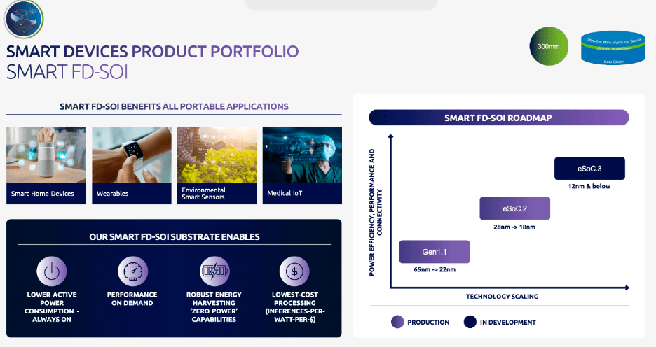
I have written before about SiC substrates to enable power electronics for EVs and EV charging stations. SOITEC offerings also include SOI (silicon on insulator), POI (piezoelectric on insulator), and GaN (gallium nitride). Each builds on an insulation layer immediately below a thin semiconductor layer on which devices are patterned. This structure eliminates (or largely eliminates) the leakage through bulk silicon, a challenge which became limiting for mainstream semiconductor processes.
Other technologies have been developed, such as FinFET, to reduce leakage though in different ways. However those processes are more complex, resulting in higher wafer costs and therefore unit device costs.
Architects and firmware designers can also minimize leakage by turning off sections of a chip when not active. This method is effective, but design requires great care to ensure that dependencies between different aspects of functionality in the chip can be cleanly separated. If shortly after turning off a powered-down section it must turn on again to service some overlooked requirement, no power is really saved. Worse still, powering down and powering back up takes time, first in delays to turn off to allow time for dependent functions to complete. And later when turning back on to first recover to the same internal state in the function right before it powered down. All this overhead adds latency and reduces true performance for the device.
SOI technologies with inherently very low leakage can more fully exploit conventional sleep modes such as clock gating and DVFS than can non-SOI technologies. These techniques result in much simpler and lower latency demands on transitions between sleep and wake modes. And because the process is less complex than other advanced processes, SOI is intrinsically more efficient in inferences/watt/$.
Interested? You can learn more HERE.
Share this post via:


Comments
There are no comments yet.
You must register or log in to view/post comments.