![]()
The crystalline structure of silicon delivers the incredible capabilities that have fueled the exponential increases defined by Moore’s Law. It turns out that silicon in its purest form will fall short at times – power handling and speed are examples. In these cases, adding additional materials to the silicon can enhance its capabilities for demanding requirements. Called compound semiconductors, these enhanced materials unlock many of the high-performance applications that are emerging today. But adding an epitaxial layer of new material to silicon is very difficult, even unpredictable at times. But an innovative company has changed all that. Read on to see how Soitec is engineering the future of the semiconductor industry.
Soitec – A Brief History
The semiconductor supply chain is a highly complex, multi-national web of organizations and capabilities. If we trace that supply chain back to its roots, we find the raw material used to manufacture semiconductor devices. This is where Soitec lives. Born out of Grenoble’s CEA-Leti (Atomic Energy Commission/Electronics and IT Technology Laboratory) in the 1990’s, Soitec has become a critical source of engineered substrate materials for the entire semiconductor industry.
With state-of-the-art manufacturing facilities in France, Belgium, Singapore, and China, Soitec has become a global leader in engineered substrates. Using its unique Smart Cut™ process, Soitec can reliably and cost-effectively insert an insulating layer between two layers of silicon oxide, creating silicon-on-insulator (SOI) wafers. One of these layers contains the differentiating materials that delivers the required improvements in system performance.
Depending on the materials used, these engineered substrates can deliver enabling performance for RF, power and optical communications as examples. Using its Smart Cut process, Soitec has an ambitious plan for heterogeneous material combinations to deliver an anything-on-anything roadmap.
The possibilities for such a roadmap have broad implications for the entire semiconductor industry. Let’s look at the impact silicon carbide (SiC) compound semiconductors have on the automotive market.
Connecting the Automotive Ecosystem with SiC Manufacturing
This was the title of a presentation Soitec gave at the recent Semicon West event in San Francisco. The presentation focused on the powertrain for EVs and the impact silicon carbide material can have there. Powertrain elements examined included:
- Electric Motor (and e-transmissions)
- Battery Pack (modules, cells, battery management)
- Power Electronics (E-drive/inverter (DC/AC), DC/DC converter, on-board charger (AC/DC))
These elements can add up to over $10,000 of system cost. The use of silicon carbide can have a big impact on these elements. When compared to traditional silicon material based on insulated-gate bipolar transistors (IGBTs), the following substantial improvements are possible:
- ~50 percent faster charging time
- ~5% – 10% increased range
- ~$500 – $1,000 reduced system cost
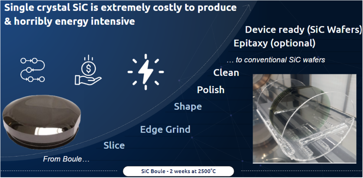
So, the question becomes what is the best path to these improvements? It turns out silicon carbide compound semiconductor material is costly, energy intensive and time-consuming to produce. To manufacture a boule of SiC which will contain 40-50 wafers each, there are many process steps that must be carefully controlled. The whole process can take about two weeks at high temperature of 2500°C which is roughly the temperature at the surface of the sun. Soitec presented the diagram below to summarize the requirements.

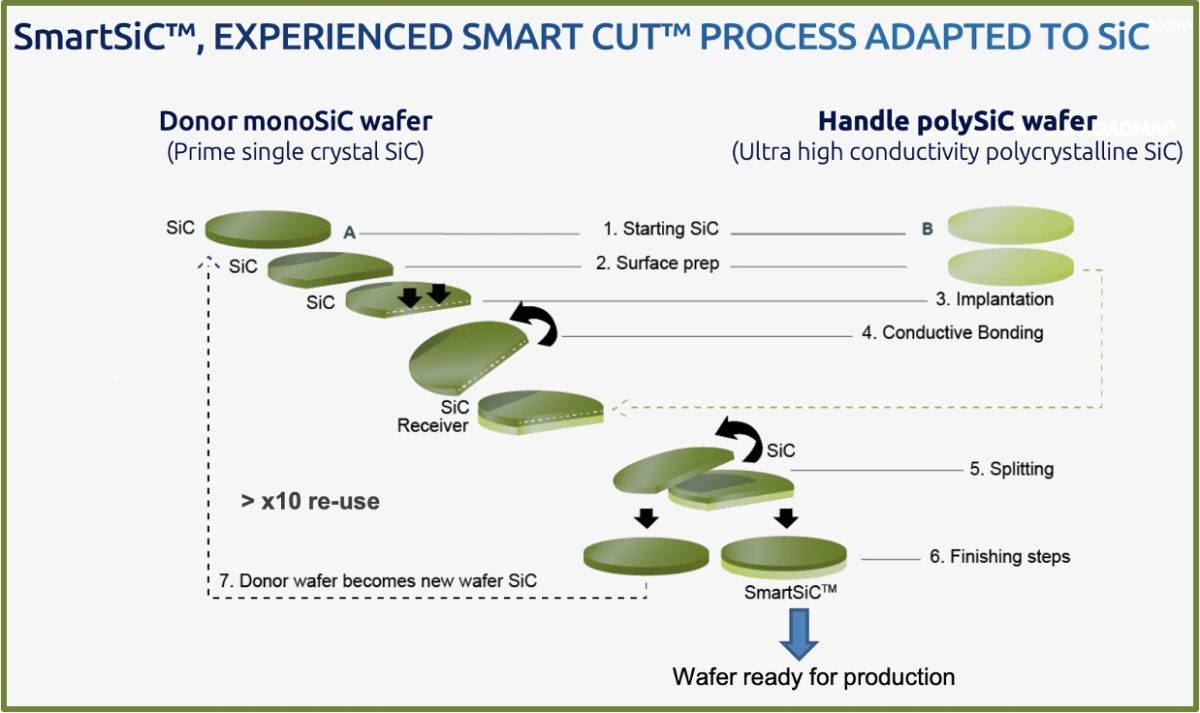
The presentation then gave a glimpse into how real Soitec’s anything-on-anything roadmap is. Using the fundamentals of its Smart Cut™ process, Soitec has created a SmartSiC™ engineered substrate. Soitec’s SmartCut™ process – think of it as an atomic scalpel – transfers an ultra-thin single crystalline SiC layer extracted from a silicon carbide so-called donor wafer, which is then bonded to an ultra-low-resistivity polycrystalline silicon carbide wafer. The donor wafer can then be re-used 10 times, said Emmanuel Sabonnadiere, vice president, automotive and industrial at Soitec, which makes this new engineered substrate unrivalled.
The benefits of this process are substantial and include:
- 40,000 tons of CO2 reduction for each 1 million wafers
- 200mm scalability to accelerate SiC adoption through 10x reusability
- Enable a new generation of SiC devices thanks to an RDSON improvement of up to 20%
- ~8X improved conductivity compared to a conventional single crystal SiC
- Reduced Capex & Opex
The figure below shows the details of the process.

Strategic partnerships are being set up across the automotive supply chain to deliver on the substantial benefits of this approach.
Comments From the Presenter

Emmanuel Sabonnadière, Vice President Division Automotive & Industrial at Soitec was the presenter at Semicon West. I had the opportunity to chat with him for a bit on the work being done at Soitec and its implications.
He began by explaining that the automotive division at Soitec has grown by 80% over the past year. Impressive. Emmanuel clearly has a passion for the impact that silicon carbide can have on system cost and performance. He has a history dating back as CEO of CEA-Leti where a lot of the early innovation occurred.
He discussed the extreme efficiency of Soitec’s process – a silicon carbide layer is complex and challenging to produce and can be used many times to create engineered substrates resulting in a highly sophisticated process.
Emmanuel also described the substantial investment being made by Soitec to build out the manufacturing infrastructure needed to broadly deploy its capabilities in the fast-growing EV market. Opening to celebrate first production is planned for end of September 2023
To Learn More
Soitec has developed a short, under two-minute video that puts all the benefits of the SmartSiC process in perspective. I highly recommend to have a look, you can find the Soitec video here. This will help you understand how Soitec is engineering the future of the semiconductor industry.
Share this post via:


Comments
There are no comments yet.
You must register or log in to view/post comments.