



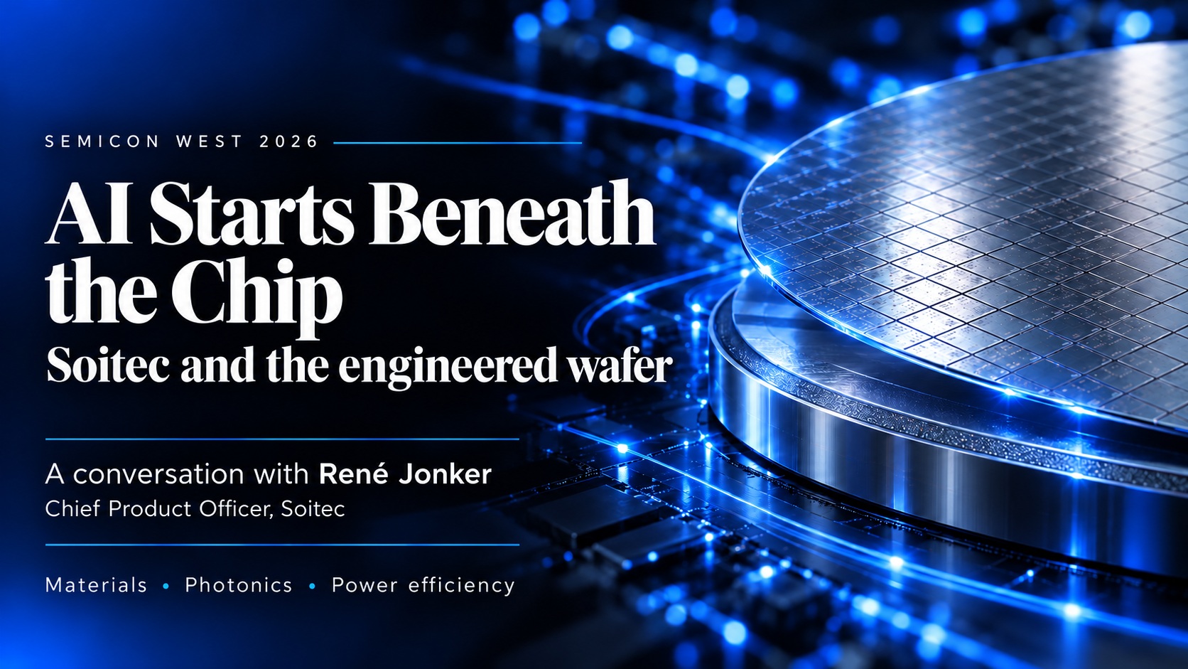
Most of the AI conversation stops at the chip. At SEMICON West 2026 I sat down with René Jonker, Chief Product Officer of Soitec, to talk about what sits underneath it.
Ask an engineer where AI performance comes from and you will hear about process nodes, dataflow, HBM stacks and interconnect fabrics. Rarely about the wafer. Yet a Grenoble company that most people outside the industry have never heard of has quietly built its business on a simple idea: if you engineer the right properties into the starting material, the foundry does not have to fight physics later.
The market has noticed. Soitec trades on Euronext Paris, and an investor who put $100 into its stock in January 2026 was holding more than $600 by early October. So I opened with the obvious question: what is the secret sauce?
A thirty-year bet on one cut
Soitec was spun out of CEA-Leti in 1992 to commercialize Smart Cut, a process that uses ion implantation and wafer bonding to slice a layer of monocrystalline silicon only nanometers thick and transfer it onto an insulating substrate. The result is silicon-on-insulator (SOI), and the name of the company says the rest.
The road was not straight. Early growth came from SOI supply deals with AMD and IBM for high-performance computing. Dependence on a few customers, and a detour into solar, brought turbulence in the 2000s. The 2010s brought the turnaround, when restructured leadership went back to the core and found its killer application: RF-SOI for smartphone front-end modules.
Soitec is neither a foundry nor a fabless designer. It sits at the very bottom of the value chain. Foundries and IDMs such as TSMC, GlobalFoundries, STMicroelectronics, Samsung Foundry and UMC buy its wafers as starting material. Fabless companies such as Qualcomm, Apple, Broadcom, MediaTek and NXP specify Soitec platforms in their designs, and the foundries follow.
That position matters more every year. As transistor scaling runs into leakage, parasitic capacitance and thermal limits, bulk silicon becomes the bottleneck. A buried oxide layer under a thin film of silicon attacks those problems at the material level, often cutting power by 30 to 50 percent without a node shrink.
Built into the starting material
Jonker puts the formula in one sentence. “By providing a substrate, you can add properties to silicon at a very early stage. Rather than having a foundry do very complicated things to get similar performance, your starting material already has certain features built in.”
RF-SOI is the proof. By eliminating the parasitics of bulk silicon, it displaced competing technologies in mobile front-end modules and turned Soitec from a small player into the dominant supplier. Today it sits in RF switches and low-noise amplifiers in practically every 5G phone and Wi-Fi module.
“The RF-SOI revolution that made Soitec an established player in substrates is a little bit behind us now,” Jonker says. What Soitec discovered is that the same toolbox can make many kinds of substrates. The company now runs five main technology platforms, each built to solve a problem that is hard to fix further down the chain.
Light becomes the new gold
The platform carrying Soitec today is one it developed a decade ago: Photonics-SOI.
“It’s now seen as the new gold,” Jonker says. The AI build-out has created a new problem: connecting the clusters. Copper runs out of bandwidth, so traffic moves to fiber. But somewhere electrons must become photons, and that interface is where Photonics-SOI lives, letting designers build optical waveguides in a silicon-based infrastructure. It is driving Soitec’s business “with a very impressive growth rate,” and it underpins the co-packaged optics now coming into AI data centers.
Positioned between mature RF-SOI technology and present-day Photonics-SOI lies a vast middle ground. FD-SOI, fully depleted SOI, cuts leakage and therefore the power of compute units, with back-biasing to trade speed against power on the fly. Automotive radar, IoT microcontrollers and edge devices use it. “I were a watch (a typical edge-device) that has FD-SOI in it,” Jonker adds. Power-SOI handles high-voltage automotive and industrial circuits, and Piezoelectric-on-Insulator (POI) targets acoustic RF filters for 5G and 6G.
Beyond silicon
The bigger shift, in Jonker’s view, is the role of materials itself. “Up until more recently, semiconductor technology was all about scaling to smaller transistors in silicon.” Now demand is growing for highly specialized materials, from gallium nitride to silicon carbide, that enable features classical silicon cannot. “That will not stop. For me it is very clear: we are progressing into the integration of heterogeneous materials.”
Soitec is positioning for it. SmartSiC reuses a single-crystal silicon carbide donor wafer many times over, bonding a thin layer onto a conductive base, which lowers the cost of SiC power devices for EV inverters. RF-GaN on insulator is in development for 6G power amplifiers and aerospace. And FD-SOI is moving to smaller geometries to serve energy-conscious on-device AI in phones and wearables.
Two kinds of competition
“For Soitec, as a substrate provider, there are two kinds of competitors,” Jonker explains. Direct competition comes from companies that provide similar engineered substrates. Indirect competition comes from competing technologies.
The more interesting competition is between technologies. An FD-SOI customer could instead choose FinFET. “FinFET technology delivers very powerful compute, but is less suitable for battery-powered devices,” he notes. A designer building a battery-powered edge device has a reason to pick FD-SOI. The two are not identical, but the end customer has a choice.
Photonics has the same tension. Silicon is “an okay material” for waveguides. Indium phosphide is better on performance and offers active photonics such as lasers, optical amplifiers and electro-absorption modulators (EAMs). But silicon wins on scaling: “The whole industry is basically set up for silicon, and indium phosphide is a more difficult material to begin with.”
The view from the bottom of the stack
That last point sums up Soitec’s position. Its substrates rarely win on raw physics alone. They win because they bring a new property into a manufacturing world built for silicon, at the one point in the chain where it is cheapest to add.
For thirty years that was a niche story. In the AI era, where every watt and every bit moved between chips counts, the wafer is becoming a design decision. Jonker’s bet is that the materials list will only get longer, and that the company holding the cut will be there when it does.
Also Read:
Power-SOI: The Reliability Engine Behind Functional Safety ICs
Apple’s iPhone 17 Series 5G mmWave Antenna Module Revealed to be Powered by Soitec FD-SOI Substrates
FD-SOI: A Cyber-Resilient Substrate for Secure Automotive Electronics
Share this post via:


Comments
There are no comments yet.
You must register or log in to view/post comments.