





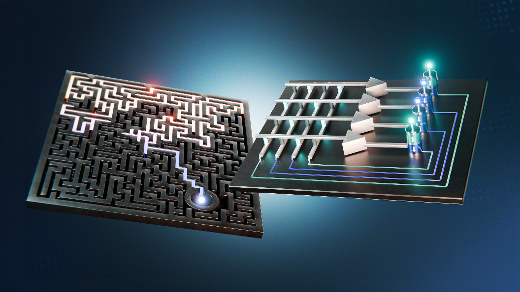
French researchers have demonstrated a hybrid nanoelectronic “Ising machine” designed to solve difficult combinatorial optimization problems more efficiently. The experimental system combines two emerging device technologies—resistive memory and spintronics—to perform parts of an optimization algorithm through the natural physics of its components, potentially reducing the energy and time consumed by conventional processors.
The work was conducted by researchers from CEA-Leti and Spintec in Grenoble and the Centre for Nanoscience and Nanotechnology at Université Paris-Saclay. Reported in Nature Communications, the project combines hafnium-oxide resistive random-access memory, or ReRAM, with stochastic magnetic tunnel junctions, known as SMTJs. The published paper describes the resulting system as an Ising machine with “intrinsic annealing.”
Combinatorial optimization involves selecting the best solution from an enormous number of possibilities. Examples include finding an efficient delivery route, scheduling factory operations, balancing an electrical grid, assigning computing resources and designing integrated circuits. Such problems become extremely demanding as their size increases because the number of possible configurations can grow exponentially.
An Ising machine reformulates an optimization problem using binary variables resembling magnetic spins, each of which can occupy one of two states. Relationships between those variables encode the problem’s constraints and objectives. The machine repeatedly changes their states, seeking a configuration with the lowest overall “energy.” That low-energy state corresponds to an optimal or near-optimal answer.
The French prototype divides this work between two complementary technologies. ReRAM devices store the weighted connections that describe how variables influence one another. Because a ReRAM crossbar can perform analog matrix operations where data are stored, it can reduce the costly movement of information between memory and a processor. The SMTJs represent the binary variables. Driven by thermal noise, they naturally fluctuate between states, providing the controlled randomness needed to explore potential solutions.
That randomness is central to the innovation. An optimizer that always moves directly downhill can become trapped in a local minimum—a solution that appears good nearby but is inferior to another configuration elsewhere. Annealing begins with stronger fluctuations, allowing the system to escape such traps, and then gradually reduces them so the variables settle into a stable answer.
In this architecture, the researchers control that process by adjusting a single read voltage applied to the ReRAM array. As the voltage changes, the influence of the stored problem progressively dominates the SMTJs’ thermal fluctuations. The hardware therefore produces an annealing schedule through the direct interaction of its components, requiring less elaborate control circuitry.
The proof-of-concept machine consistently reached the global optimum in a 24-vertex weighted MAX-CUT benchmark and a 10-vertex, three-color graph-coloring problem. It operated at room temperature without an applied magnetic field—important practical conditions for eventual integration. The researchers also emphasize that ReRAM, magnetic tunnel junctions and CMOS circuitry are compatible with back-end-of-line fabrication and vertical three-dimensional integration. CEA-Leti’s announcement presents the experiment as a step beyond demonstrations of isolated devices.
Why does it matter? Much of modern computing’s energy is spent moving data and executing instructions rather than performing essential arithmetic. This machine instead stores problem coefficients, generates randomness and updates variables close to—or directly through—the devices themselves. A mature implementation could become a compact accelerator for optimization-intensive workloads.
Bottom line: This remains a small experimental prototype, not evidence of superiority over leading conventional solvers. Updates are currently sequential, external feedback is still used for measurement, and comparative speed and energy benefits have not yet been quantified. The next tests must integrate control electronics, operate variables in parallel, scale to substantially larger problems and benchmark complete systems fairly. If those challenges are overcome, nanosecond switching and direct device coupling could turn this hybrid architecture into a valuable, highly efficient companion to general-purpose computers.
Also Read:
Designing chips for the AI era: what TSMC’s roadmap means
The Intelligence Revolution: TSMC’s OIP Ecosystem Forges the Path to Trillion-Transistor AI Systems
Podcast EP368: An Overview of TSMC Open Innovation Platform (OIP) event with Aveek Sarkar
Share this post via:


Why America’s Semiconductor Manufacturing Capacity Matters