You are currently viewing SemiWiki as a guest which gives you limited access to the site. To view blog comments and experience other SemiWiki features you must be a registered member. Registration is fast, simple, and absolutely free so please,
join our community today!
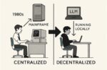
The PC industry is entering its most significant transformation since the debut of the IBM PC in 1981. That original beige box ushered in a new era of productivity, reshaping how corporations and individuals worked, communicated, and created. More than four decades later, the AI PC is emerging as a new category — one that promises… Read More
Can cash and IBM collaboration put Japan into premier-league chipmaking? Rapidus is betting billions it can.
When Japan announced the creation of Rapidus in 2022, the news was met with a mix of enthusiasm and skepticism. The company would enter the market at a time of escalating demand for semiconductor fabrication capacity to… Read More
When I do a root cause analysis of Intel’s problem it is very simple. If Intel wants to continue to be a leading-edge semiconductor manufacturer, they need to fill their fabs, all of their fabs. Clearly several things need to happen in order to do that but the one that most interests me is on the foundry side.
I think we can all agree that… Read More
Many of you are already familiar with Silicon Catalyst and the value it brings to semiconductor startups, the industry and the electronics industry at large. Silicon Catalyst is an organization that supports early-stage semiconductor startups with an ecosystem that provides tools and resources needed to design, create, and… Read More
One of the recent live events I attended was the 2022 GSA Silicon Leadership Summit on May 12th at the Santa Clara Convention Center (my favorite location). This was the first GSA live event in two years so it was a must attend gathering. This event targets semiconductor ecosystem executives (200+ people attended) so there were many… Read More
Dan is joined by Terry Daly, a 35-year veteran of the semiconductor industry, former senior VP at GLOBALFOUNDRIES and an executive at IBM Microelectronics. Terry is currently an independent consultant, and also a Senior Fellow at the Council on Emerging Market Enterprises at The Fletcher School of Law & Diplomacy at Tufts… Read More
I spent several days this week at the SEMI International Strategy Symposium (ISS). One of the talks was “Can the Semiconductor Industry Reach $1T by 2030” given by Bob Johnson of Gartner. His conclusion was, that $1 trillion dollars is an aggressive forecast for 2030 but certainly we should reach $1 trillion dollars in the next 10… Read More
IBM at IEDMby Scotten Jones on 01-10-2022 at 6:00 amCategories: Events
IBM transferred their semiconductor manufacturing to GLOBALFOUNDRIES several years ago but still maintains a multibillion-dollar research facility at Albany Nanotech. IBM is very active at conferences such as IEDM and appears to have a good public relations department because they get a lot of press.
At the Litho Workshop … Read More
The field of DRAM is fascinating as it continues to grow and innovate. For the past ten years, I have often read that DRAM is running out of steam because of its difficulty to scale the capacitor, and yet it continues to evolve since invented by Dr. R. Dennard at IBM. In 1966, he introduced the concept of a transistor memory cell consisting… Read More
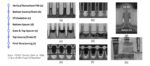
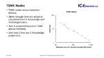
IBM has announced the development of a 2nm process.
IBM Announcement
What was announced:
- “2nm”
- 50 billion transistors in a “thumbnail” sized area later disclosed to be 150mm2 = 333 million transistors per millimeter (MTx/mm2).
- 44nm Contacted Poly Pitch (CPP) with 12nm gate length.
- Gate All Around (GAA), there are several ways
…
Read More