





By Vignesh Sunderrajan
Every physical design engineer knows the moment. The implementation run finishes with reasonable Worst negative slack (WNS) and total negative slack (TNS) is insignificant. Then the sign-off static timing analysis (STA) run lands and reports violations that place-and-route (P&R) never showed.
Nothing in the design changed between those two runs. The two environments described the same circuit with different models. The difference between their answers has a name. It is the convergence delta, and I have spent most of my career on the implementation side of it, leading P&R and timing closure on high-frequency low power CPU blocks and networking ASICs, and building flows to make the two environments agree earlier.
A convergence delta is the difference between the slack the implementation environment reports and the slack sign-off STA reports for the same path, in the same design and stage. It is measured path by path, in picoseconds, and it has a sign. A path can come out Y ps better in sign-off, or Z ps worse.
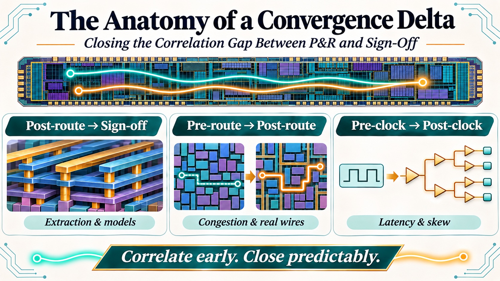
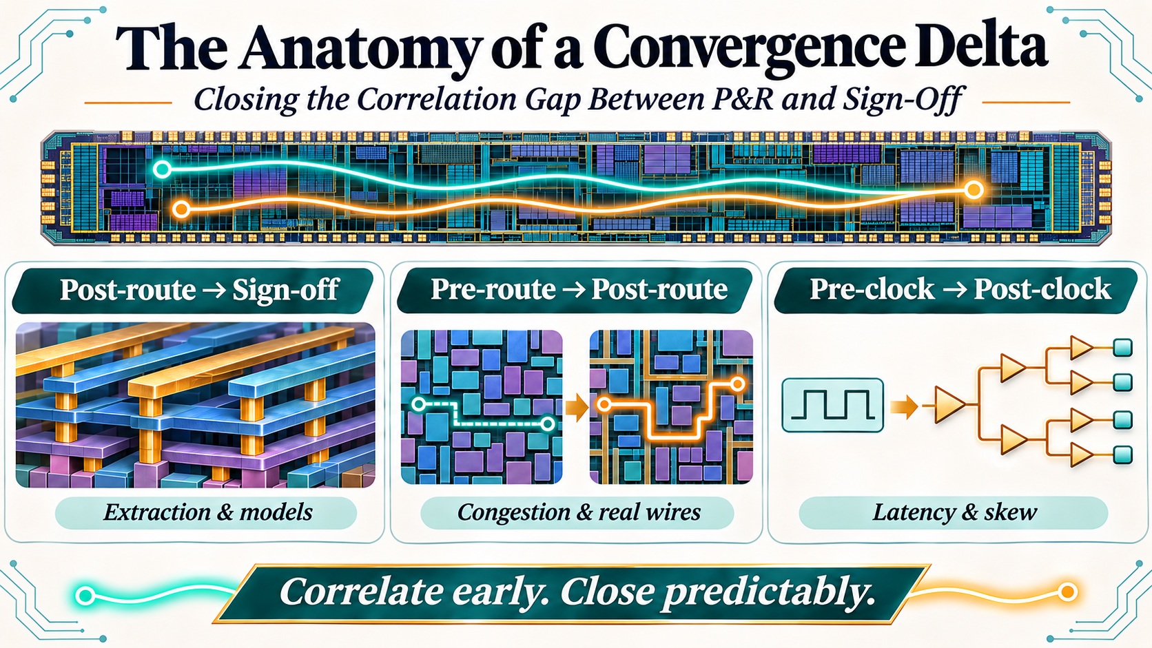
The wrong response is to chase absolute markers inside the local tool: a WNS target hit in P&R means little when sign-off reads the same layout differently. Work instead for relative improvements across the P&R stages that translate predictably to sign-off, across three transitions with three different correlation profiles. Pre-route numbers rest on placement approximations, post-route numbers meet a far more exact extraction engine, and pre-clock numbers assume a clock that does not exist yet.
Two runs can report different WNS and paths move in different directions underneath it. The mode of comparison has to be the paths between the different P&R and signoff – i.e., for the same startpoint, same endpoint, same corner, slack read from both environments. This could give guidance to the next P&R run.
Plot the delta as a histogram. A tight distribution shifted by near constant offset points at a global setting: derates, a corner definition, a library version. A wide spread with a long tail points at extraction on specific nets or at the clock network. Then split the delta between the P&R tool and signoff into various components that would help capture the key reason for the delta. The split, consisting of various components that indicate the reason for the delta, decides the fix, so do it before iterating over the design in the P&R world.
Puzzle 1: the post-route to sign-off bridge (the physics of extraction)
During optimization, the internal tool calculates timing with fast parasitic approximations. It repeats that extraction thousands of times, so it trades accuracy for runtime. Sign-off extraction makes the opposite trade: it parses the finished layout in full three-dimensional detail, covering metal thickness, line spacing, neighbor-to-neighbor coupling capacitance, metal fill, and via stacks across advanced lower nodes interconnect profiles. The same net gets two different resistance and capacitance values, and every path through that net inherits the difference. A layout clean inside P&R can fray into late-stage timing and signal integrity violations at this boundary, because the internal numbers are rough indicators, and treating them as exact breeds false confidence.
The working method is comparison, early and net by net. Run the implementation extractor on a routed block with similar coupling and fill settings the sign-off extractor uses, and compare extracted values on a sample of long routes. Tune the implementation settings until the sample agrees within a small margin, then freeze both sides. Past that point, stop chasing exact mimicry. It is computationally out of reach, and the attempt eats runtime the schedule does not have. Experienced block owners work with systemic offset margins and directional trends instead: they track how a change in wire spacing or driver sizing inside the layout flow shows up in sign-off reports, and keep the design moving toward closure.
Delay calculation differs between engines: cell delay and output slew get interpolated differently over the same library tables, input pin capacitance is treated differently, and crosstalk delta delay enters one engine’s numbers while the other skips it during optimization. Per stage, the difference could be a few picoseconds. Across a deep stage path, it is a budget item. Libraries and corners drift, too. The implementation flow optimizes against a handful of scenarios, and sign-off checks more of them, sometimes with a newer library release, sometimes at a voltage or temperature point the implementation list never included.
On-chip variation derating is the easiest source to get wrong. It lives in setup files and moves every path at once. If the implementation flow applies a particular percent derate to data paths and sign-off applies another, every path shifts by the difference, and the shift grows with path length. Derates applied to the clock network in one environment and skipped in the other move setup and hold in opposite directions.
Puzzle 2: the pre-route to post-route continuum (virtual wires vs. physical reality)
Move one transition upstream and the delta widens. At the placement stage, no real wires exist. The optimization engine relies on virtual routing models, global route grids, and wire-load approximations. Those models are clean. Physical routing is not.
Placement engines are rewarded for worst-case timing improvements measured against the virtual model, and one cheap way to shorten a critical datapath on paper is to pack its cells tightly into a compact area. The detailed router then has to pass thousands of signal nets through that same crowded space. Layer assignments, via stacks, and localized track blocking force long detours around macro blocks, and actual wire capacitance and resistance climb far past the placement engine’s estimates. The placer set a physical trap, and the router pays for it.
Resolving this puzzle is a reading habit: pre-route congestion maps and the growth of the TNS population are early indicators of post-route reality. A path group whose negative slack keeps spreading across more endpoints at placement is telling you what detailed routing will confirm later, and a region running hot on the congestion map will produce detours that no virtual model predicted. Distributed cell utilization bounds stop it from filling every region to the same density, and localized padding around certain edges and known choke points leaves room the router will need. Both cost a little area and pre-route slack on paper, and buy back far more after routing, when the wires are real. Judge a placement by how its numbers survive that transition, because a pre-route gain bought with density usually arrives at sign-off as a loss.
Puzzle 3: the pre-clock to post-clock shift (idealism to network insertion)
The third transition sits at clock tree synthesis (CTS). Pre-clock timing analysis works in a state of idealism. Clock signals are assumed to launch and capture with zero skew, zero delay, and perfect synchronicity, so data paths get optimized against a flat, uniform baseline.
CTS ends that arrangement by physicalizing the network. Clock buffers, dividers, and distribution trees go in across the block and around the macro arrays. The inserted network brings real insertion delay and localized clock skew, driven by on-chip variation, voltage drops, and metal layer changes. Data paths that closed easily during placement can blow past their setup or hold budgets at that point, because their clock arrival times have physically shifted.
Mastering this transition means making the post-clock network visible before any clock buffer is placed. Configure the pre-CTS environment with realistic, data-driven clock latency and skew models that match the targeted clock distribution topology’s physical footprint, and hold data paths to skew budgets drawn from that topology during placement and pre-route optimization. Paths built under those assumptions arrive at CTS with margin for the insertion delay and skew the real network is about to add, and the post-clock reports confirm the pre-clock ones.
Conclusion: the unified correlation map
Read the pipeline as one continuous map of data transitions: pre-clock to post-clock, pre-route to post-route, post-route to sign-off. Decisions made under ideal conditions cascade through all three transitions. The engineer who holds the whole map stops reacting to late-stage errors and starts steering each stage by what the next stage will do to its numbers.
Model sign-off checks inside the implementation flow in the early PNR stages so that fixes are still cheap. The key idea is to move the argument earlier and make the necessary changes in the implementation flow and a rerun could still settle it. A delta found after detailed routing gets a harder reception: placement is frozen, routing channels are full, and the fix becomes ECO work. I have implemented various late-stage functional ECOS cycles on on designs and held PPA flat through them. When designs are built from the start with robustness and predictability alongside power, performance, and area (PPA), even late-stage functional ECO cycles can be absorbed while holding PPA flat.
About the Author Vignesh Sunderrajan
I am a silicon design professional with fifteen years of experience implementing high-performance mobile, laptop, and networking chipsets, contributing to complex CPU and SoC programs from RTL to final layout at advanced technology nodes. I hold a Master’s degree in Electrical Engineering from Stanford University, specializing in Circuit Design and VLSI, and I am a Senior Member of the IEEE.
Also Read:
CTO Interview Kevin Robinson, VP of Operations, yieldHUB
CXO Interview with Solaiman Rahim of ChipAgents
Golden Testcases You Can Check With a Calculator
Share this post via:


NVHBM: Can Custom HBM Change Who Builds the Memory Stack?