


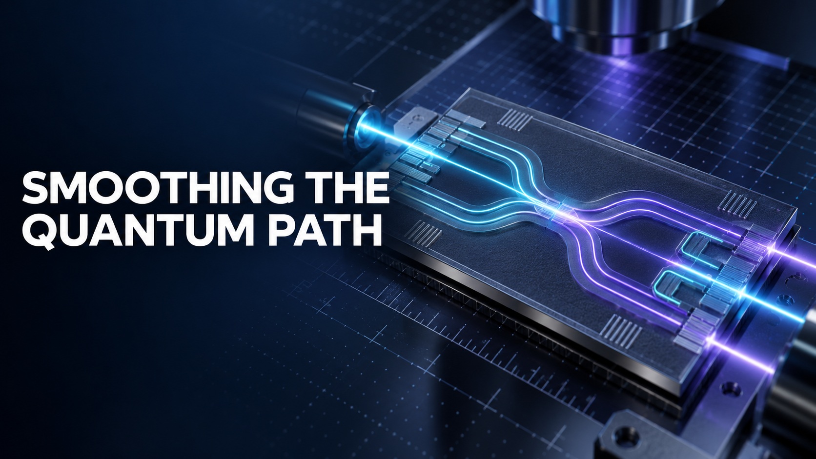


ASML’s decision to collaborate with Xanadu targets one of photonic quantum computing’s most unforgiving engineering constraints: photon loss. The companies will investigate advanced lithography processes for Xanadu’s photonic quantum hardware, focusing on whether tighter patterning control can suppress loss mechanisms and improve the prospects for fault-tolerant, utility-scale machines.
Photonic quantum processors encode and manipulate quantum information in states of light. Their appeal is substantial: photons move quickly, interact weakly with the environment and can support room-temperature system architectures. Xanadu combines sources, interferometers, switches, detectors and optical interconnects to generate and process entangled states. Yet the same weak interaction that protects photons from environmental noise makes lost photons difficult to recover. Absorption, scattering, imperfect coupling and component inefficiency can remove carriers of quantum information before computation is complete.
Loss compounds rapidly as circuits grow. If a photon survives each of N sequential components with probability η, the end-to-end survival probability scales approximately as η^N. Even a small per-component penalty therefore becomes severe in deep circuits. Lost photons reduce successful sampling rates, degrade entanglement and consume error-correction resources. Fault-tolerant architectures can tolerate finite loss, but only below architecture-dependent thresholds and with considerable overhead. Better fabrication attacks the problem at its physical source.
The ASML-Xanadu program specifically connects optical loss with line-edge roughness, or LER. Lithography defines the lateral boundaries of waveguides and other nanophotonic structures. Real edges contain nanoscale deviations from the intended geometry because of exposure, resist chemistry, development and pattern-transfer effects. These deviations perturb the waveguide’s refractive-index boundary, coupling guided light into radiation modes or producing back-scattering. The resulting propagation loss is especially consequential when light traverses long routes, resonant structures or many repeated components.
Reducing LER is not simply a matter of printing smaller features. Engineers must optimize the full patterning stack: exposure conditions, mask design, resist selection, stochastic variability, etch bias, sidewall profile and process control. Critical-dimension uniformity also matters because variations shift optical phase, splitting ratios and resonance frequencies. A process can meet nominal linewidth targets yet still deliver poor quantum performance if edge spectra, sidewall angles or wafer-scale uniformity are uncontrolled.
ASML brings expertise in lithographic imaging, process windows, metrology and computational correction. Xanadu contributes device requirements, photonic circuit designs and quantum-level performance data. Together, they can connect manufacturing variables to optical figures of merit rather than treating lithography and quantum architecture as separate optimization problems. Useful experiments could correlate measured LER power spectra with waveguide attenuation, quantify sensitivity to pattern-transfer steps and establish design rules that trade density against loss and yield.
The collaboration does not mean ASML is building a quantum computer, nor does the announcement specify a production node, tool platform or numerical loss target. It is a research effort to understand which lithography-enabled approaches can produce lower-loss photonic structures. That distinction matters: ultra-fine resolution alone does not guarantee smooth interfaces, and laboratory improvements must ultimately transfer to stable, high-yield manufacturing.
Commercially relevant photonic quantum systems will require repeatable fabrication across many dies, modules and wafers. Variability that is acceptable in classical photonics may be costly when thousands or millions of optical operations contribute to one error-corrected computation. Process improvements can create system-level leverage by increasing photon survival, reducing calibration burden and lowering the number of physical resources required per logical qubit.
Success will also depend on packaging, fiber-to-chip coupling, detector efficiency and source quality, which lithography cannot solve alone. Still, lowering on-chip propagation and component loss expands the available system budget, making every downstream engineering compromise easier to manage at scale.
Bottom line: The partnership therefore links semiconductor manufacturing discipline with quantum error-correction economics. If advanced lithography can measurably reduce scattering and device variability, Xanadu may obtain more reliable photonic building blocks, while ASML gains insight into requirements beyond conventional electronic scaling. The immediate outcome is process knowledge, not a finished fault-tolerant machine. But for photonic quantum computing, lowering each fraction of a decibel can translate into a disproportionately larger and more useful processor.
Also Read:
High-NA EUV Moves From Experiment to Manufacturing
ASML and TSMC’s 12-Inch Photomask Initiative: Technical Significance
Five Billion Pulses Later: What DUV Optics Testing Reveals About Semiconductor Tool Uptime
Share this post via:


Rethinking Phase Jitter: An Algorithmic Approach to Signal Integrity