







EUV has long been an interesting story. We have written 200+ articles on EUV and they just keep on coming. Thankfully the premier lithography conference is right here in Silicon Valley. SPIE began in 1955 as the Society of Photographic Instrumentation Engineers, bringing together engineers using scientific cameras and high-speed photography for measurement and research. Its scope grew alongside advances in lasers, imaging and optical technology.
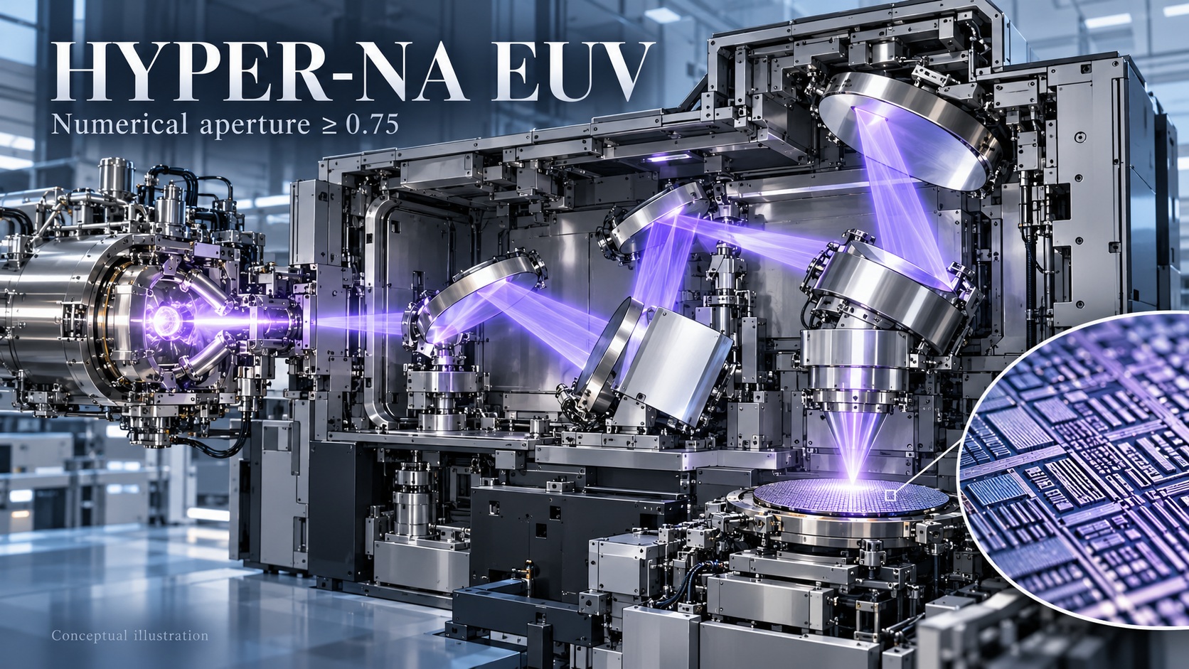
The semiconductor industry’s future depends partly on how precisely it can print the circuitry inside a chip. Hyper-NA, an emerging concept for extreme ultraviolet lithography, would push that precision beyond today’s most advanced commercial systems. Its defining specification—a numerical aperture of at least 0.75—describes an optical system capable of resolving finer patterns. The opportunity is substantial: continue shrinking critical chip features while potentially simplifying their manufacture. However, Hyper-NA remains a development prospect, with no confirmed customer delivery date.
Numerical aperture, or NA, measures the range of angles over which an optical system accepts light. Increasing it improves the ability to distinguish closely spaced features. ASML’s established EUV systems have an NA of 0.33, while its newer High-NA machines reach 0.55. Both use light with a wavelength of 13.5 nanometres. ASML lists their respective resolutions as 13 and 8 nanometres. Hyper-NA would take the next step by increasing aperture while retaining the EUV wavelength.
This matters because lithography determines which patterns manufacturers can transfer onto silicon during fabrication. At a fixed wavelength and otherwise comparable processing conditions, printable dimensions decrease as numerical aperture increases. Moving from 0.55 to 0.75 therefore implies approximately 27 percent smaller dimensions through aperture alone. Actual manufacturing results also depend on illumination, masks, materials and processing. The calculation illustrates the opportunity, rather than guaranteeing a particular transistor size or commercial chip generation.
The economic attraction extends beyond smaller features. When a scanner cannot print a sufficiently dense pattern in one exposure, manufacturers may divide it into multiple patterns, adding processing and alignment requirements. ASML’s roadmap identifies an opportunity for 0.75-NA single exposure to replace some multiple-patterning applications using 0.55-NA equipment. Successful implementation could reduce manufacturing complexity on selected layers. Whether it lowers overall costs would depend on machine productivity, reliability, material requirements and the number of usable chips produced.
For users, the potential benefits would appear indirectly through future processors and memory. Finer patterning can support greater circuit density and new device designs, contributing to improvements in computing capability and energy efficiency. Those outcomes also require advances in transistor architecture, interconnects and packaging. Hyper-NA would expand the manufacturing options available to chip designers. Its significance lies in helping preserve a route toward continued scaling as existing exposure techniques approach their practical limits.
The engineering challenge is demanding. Higher aperture reduces depth of focus: the vertical range within which a projected pattern remains sufficiently sharp. Consequently, wafer surfaces, focus control and light-sensitive resist films face tighter requirements. Research on high- and hyper-NA materials highlights the need for thinner resists while controlling defects and pattern variation. A sharper optical image provides limited value if subsequent processing cannot reproduce it consistently across a wafer. Manufacturing readiness requires the entire process to work together.
When will Hyper-NA be delivered? As of October 2026, the defensible answer is that no firm shipment schedule has been announced. Reuters reported that engineers at ASML and optical partner Carl Zeiss describe potential readiness in about ten years, pointing roughly to 2036. That is a development horizon, subject to technical progress and commercial decisions. ASML has begun development but has not committed to producing the machine. Readiness, initial customer delivery and widespread factory adoption could occur at different times.
Bottom line: The industry’s nearer milestone remains High-NA deployment. ASML and TSMC have announced plans for TSMC to begin using High-NA in high-volume manufacturing in 2030, alongside an initiative targeting larger-mask system readiness for advanced production by 2033. Hyper-NA would build on that evolving infrastructure. Its importance today is strategic: it gives manufacturers another credible direction to investigate, while reminding the industry that extending chip scaling requires years of coordinated work before a promising optical design becomes dependable production equipment. The eventual decision will depend on whether its advantages justify the investment for customers.
- Research paper: “Hyper NA: a system with a numerical aperture of at least 0.75” — Michael Patra, Heiko Feldmann, Jens Timo Neumann and Gerardo Bottiglieri, October 2026. I located the paper but couldn’t access its full text.
- Reuters: ASML and Zeiss say next-generation technology may be ready in 10 years — October 8, 2026. Source for the roughly 2036 readiness outlook, which is not a confirmed delivery date.
- ASML: EUV lithography systems — Current 0.33-NA and 0.55-NA specifications and resolution.
- ASML’s 2024 Investor Day presentation — Hyper-NA roadmap and potential manufacturing benefits.
- Research on resists for High-NA and Hyper-NA EUV — Resolution, depth-of-focus and material challenges.
- ASML–TSMC larger-photomask initiative — September 8, 2026. High-NA adoption and infrastructure timeline.
Also Read:
Pollen Metrology: From a Decade-Long Bet to a Proven AI Platform for Semiconductor Manufacturing
Why ASML Is Racing to Build 110 EUV Machines
ASML Has High-NA and Chipmakers Can’t Say No
Share this post via:



Hyper-NA EUV: The Next Frontier in Chipmaking Could Arrive in 2036