





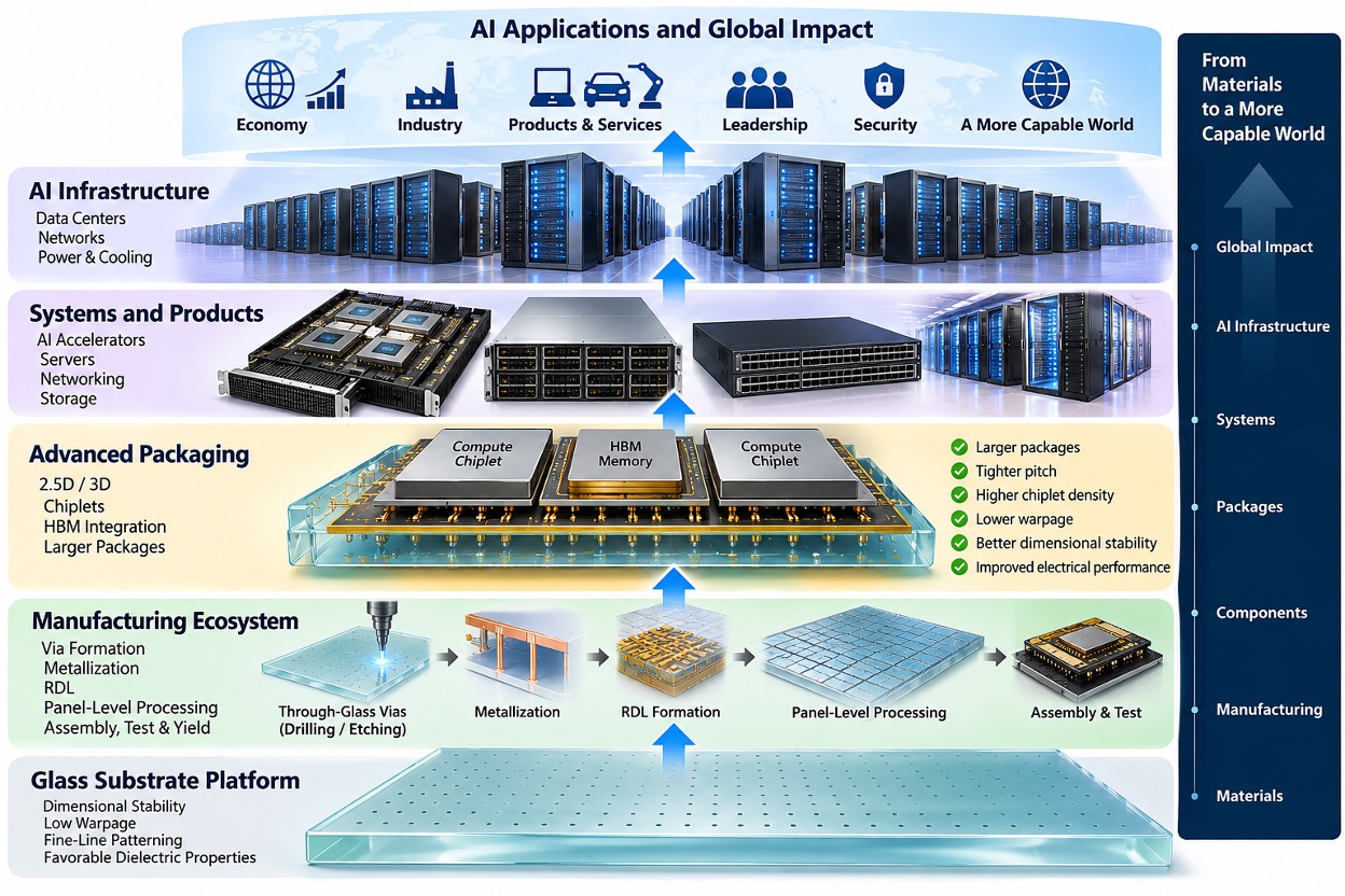
The value of glass will be determined not by its material properties alone, but by whether it can expand the package architecture window and be realized repeatedly at manufacturing scale.
AI infrastructure is pushing advanced packaging into a regime where the substrate itself increasingly determines what can be built.
As packages grow larger, chiplets move closer together, redistribution becomes finer, power density rises, and alignment and warpage margins shrink, the substrate is no longer just a passive support structure.
It becomes part of the architecture.
And that is where glass becomes potentially transformative.
The Substrate Is Becoming an Architecture Constraint
The package substrate increasingly determines:
- how large the package can become,
- how closely chiplets can be placed,
- how fine the redistribution geometry can be,
- how much warpage can be tolerated,
- how stable alignment remains during processing,
- how electrical paths scale,
- and how much integration can occur before package mechanics become limiting.
These are not isolated material questions.
They are package-geometry and interface questions.
The substrate influences the physical boundaries between die, memory, interconnect, redistribution, thermal structures, board interfaces, and assembly processes.
As AI packages become larger and more heterogeneous, those boundaries become harder to control.
That means the package process window increasingly becomes part of the architecture.
Glass Could Expand the Package Process Window
This is where glass becomes interesting.
Its potential value is not simply:
- lower warpage,
- better dimensional stability,
- fine-line capability,
- attractive dielectric behavior,
- or compatibility with large-format processing.
The deeper opportunity is that these characteristics may allow the package to operate inside a wider or more stable physical process window.
That can mean:
larger package size
→ tighter geometry
→ better registration
→ more stable interfaces
→ more predictable assembly
→ greater integration density
If that holds through manufacturing, glass does more than improve one property.
It changes what package architectures are physically realizable.
That is why glass could become an architecture-enabling platform for AI infrastructure.
AI Infrastructure Demand Is Pulling Glass Forward
AI accelerators are pushing packaging in several directions at once.
Compute die are getting larger and more powerful.
HBM is being placed increasingly close to compute.
Chiplet counts are increasing.
Electrical routing density is rising.
Thermal density is rising.
Package dimensions are expanding.
At the same time, assembly tolerances are becoming less forgiving.
That creates a fundamental tension:
the package is getting larger while the acceptable geometric error is getting smaller.
This is exactly the kind of problem where substrate dimensional stability becomes strategically important.
Glass therefore is not being pulled forward by one application.
It is being pulled by the broader physical requirements of AI infrastructure.
Dimensional Stability Becomes an AI Packaging Variable
Dimensional stability sounds like a material property.
But in advanced packaging, it quickly becomes a system variable.
For example:
lower substrate deformation
→ better die-to-substrate registration
→ more stable RDL geometry
→ improved assembly alignment
→ more predictable electrical and mechanical behavior
Or:
lower warpage
→ improved coplanarity
→ more consistent attach
→ lower variation in interconnect geometry
→ more stable product performance
That is where material behavior becomes architecture value.
The important question is not:
How stable is the glass?
It is:
What package constraints can that stability remove?
That is a much more useful way to evaluate the platform.
Glass Creates an Opportunity for the Manufacturing Industry
The opportunity is not limited to substrate suppliers.
If glass scales, it creates a broader manufacturing ecosystem around:
- through-glass via formation,
- laser drilling and etching,
- metallization,
- redistribution layers,
- fine-line processing,
- panel handling,
- inspection,
- metrology,
- assembly,
- test,
- reliability,
- and qualification.
That means glass can create new value across the packaging supply chain.
But it also creates new manufacturing challenges.
Glass must be handled differently.
Via formation has to remain uniform.
Metallization has to remain reliable.
Large panels must maintain dimensional control.
Defects have to be detected.
Interfaces have to remain stable.
Assembly flows have to account for the mechanical behavior of the complete stack.
So the manufacturing question becomes:
Can the industry control the complete process window, not just demonstrate the material?
That is where the platform either becomes real or remains experimental.
Panel-Level Processing Could Change the Economics
One of the most interesting opportunities is panel-level processing.
If glass can support large-format processing while maintaining dimensional stability, it may allow the industry to change the relationship between:
- package size,
- precision,
- throughput,
- and manufacturing cost.
That could become particularly important as AI packages continue to grow physically.
The value would not be simply “bigger panels.”
It would be:
larger-format manufacturing without losing the geometric control required by advanced heterogeneous integration.
That is a potentially important economic and manufacturing transition.
Glass Has to Prove Itself Across the Complete Package
This is where the real test begins.
Glass does not operate alone.
It has to coexist with:
- silicon,
- HBM,
- copper,
- RDL,
- solder,
- underfill,
- adhesives,
- thermal materials,
- organic build-up layers,
- connectors,
- and board-level assembly.
Every interface matters.
Glass may reduce substrate warpage but still create integration challenges elsewhere.
Its dimensional stability may be excellent, but metallization or via reliability may become limiting.
Its dielectric behavior may be attractive, but assembly interfaces must still survive thermal cycling.
Its large-format processing may look promising, but panel handling and defect control must support yield.
So the real challenge is not just material compatibility.
It is package coexistence and operability.
The question becomes:
Can glass remain beneficial after every interface, process step, thermal cycle, and assembly operation required to build the final AI package?
That is the level at which the platform must be judged.
From Material Potential to Manufacturing Reality
The maturity path matters:
R&D / Prototype
→ Pilot Production
→ Engineering Builds
→ Qualification
→ Early Commercial Production
→ High-Volume Manufacturing
Each stage proves something different.
A prototype proves the architecture can exist.
Pilot production begins to expose process variation.
Engineering builds begin to reveal repeatability.
Qualification tests whether the integrated structure survives expected stress.
Early production exposes yield behavior.
High-volume manufacturing proves the complete ecosystem can operate repeatedly and economically.
This is where glass has to make the transition from:
material capability
to:
package capability
and then to:
manufacturing capability
The Real Test of Glass
The real test is not whether glass can demonstrate impressive material properties.
It is whether glass can be realized as part of an AI infrastructure platform.
That means answering harder questions:
- Can the package remain dimensionally stable at larger scale?
- Can fine-line geometries remain controlled across production?
- Can through-glass vias and metallization maintain reliability?
- Can assembly interfaces remain within tolerance?
- Can glass coexist with silicon, copper, organics, adhesives, and thermal materials?
- Can inspection and metrology identify the defects that matter?
- Can qualification demonstrate stable behavior?
- Can yield and cost support volume production?
- And most importantly, can glass enable package architectures that would otherwise be difficult to realize?
If the answer becomes yes, then glass has moved beyond being a substrate material.
It has become part of the AI infrastructure platform.
The transition is:
material capability
→ package process window
→ package architecture window
→ manufacturing capability
→ AI infrastructure capability
That is the real opportunity.
Also Read:
From 25 Million Pixels to a Six-Ounce Product: Engineering Visor for Manufacturing
AI-EDA Agents Can Prove Their Value
Agentic AI Can Reach GDS. What Must It Prove Before Engineers Trust It for Tapeout?
Share this post via:


Intel’s Tiny Bridges Could Lead to Very Big Paychecks