You are currently viewing SemiWiki as a guest which gives you limited access to the site. To view blog comments and experience other SemiWiki features you must be a registered member. Registration is fast, simple, and absolutely free so please,
join our community today!
IC Packaging Technologyby Admin on 07-06-2026 at 7:14 pm
Integrated Circuit packaging has always been integral to IC performance and functionality. An IC package serves many purposes: 1) pitch conversion between the fine features of the IC die and the system level interconnection; 2) chemical, environmental and mechanical protection; 3) heat transfer; 4) power, ground and signal… Read More
Automatic adaptive meshing in HFSS is a critical component of its advanced simulation process. Guided by Maxwell’s Equations, it efficiently refines the mesh to accurately capture both the geometric and electromagnetic detail of a design. The end result is a process that guarantees accurate and reliable simulation results… Read More
TSMC as Pure Play Wafer Foundry
TSMC started its wafer foundry business more than 30 years ago. Visionary management and creative engineering teams developed leading-edge process technologies and their reputation as trusted source for high-volume production. TSMC also recognized very early the importance of building an … Read More
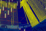
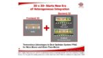
There is an emerging set of advanced packaging technologies that enables unique product designs, with the capability to integrate multiple die, from potentially heterogeneous technologies. These “system-in-package” (SiP) offerings provide architects with the opportunity to optimize product performance, power, cost,… Read More
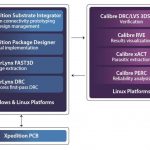
After teams sweat the details of SoC and industrial design, they turn to printed circuit board designers for magic. Here are a pile of chips and passives, and a schematic for interconnecting them. This is how much physical space the board can occupy. Connectors have to be here, and here, and mounting holes there, and there. There … Read More