






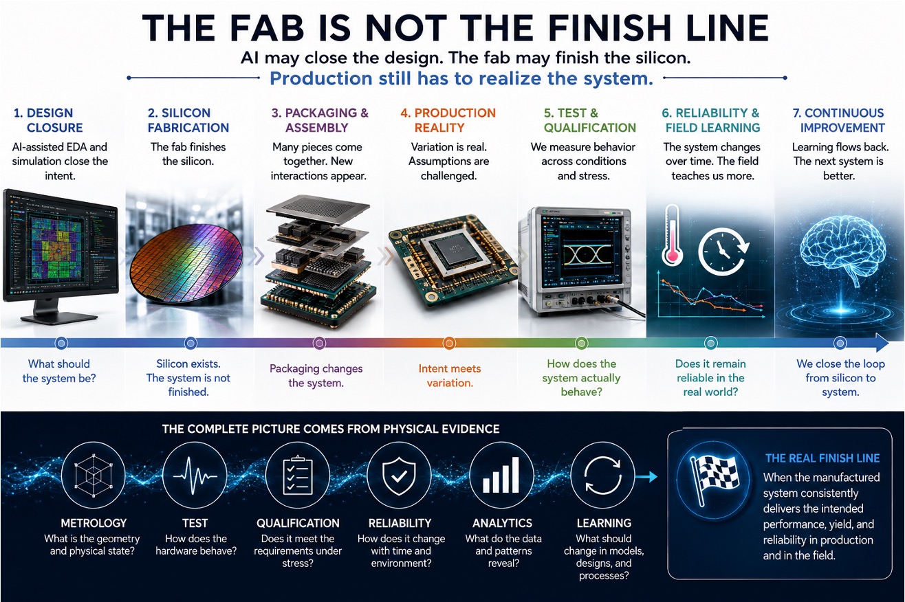
AI may close the design. The fab may finish the silicon. Production still has to realize the system.
Semiconductor engineering is becoming extraordinarily capable.
EDA platforms are expanding from individual design tasks toward increasingly complete system analysis.
Multiphysics simulation is connecting electrical, thermal, mechanical, and optical behavior.
AI-assisted engineering is beginning to automate portions of exploration, optimization, verification, and debug.
Agentic workflows may eventually coordinate increasingly complex design tasks with far less manual intervention.
Digital twins are becoming richer.
Foundries continue to push device performance, integration density, process control, and manufacturing sophistication.
These are major advances.
But there is an important distinction that can easily disappear as the tools become more powerful:
The design can be complete while the product is not.
And:
The fab can finish the silicon. It does not finish the system.
For a modern heterogeneous semiconductor product, the journey from design intent to production hardware continues long after tapeout and wafer fabrication.
Packaging, assembly, substrate behavior, interconnect geometry, materials, thermal movement, power delivery, optical alignment, manufacturing variation, inspection, test, qualification, and reliability all continue shaping what the system ultimately becomes.
That boundary is becoming increasingly important.
Design Closure Is Not Product Closure
The semiconductor industry has spent decades improving design closure.
Timing must close.
Signal integrity must close.
Power integrity must close.
Thermal constraints must be understood.
Physical implementation must satisfy increasingly complex design rules.
Verification must demonstrate that the intended logic and interfaces operate correctly.
And increasingly, AI is being introduced into these workflows.
That progress matters.
A future AI-assisted design environment may explore architectures, optimize placement, evaluate power delivery, detect violations, run multiphysics analysis, compare alternatives, and help engineers converge on a much stronger design faster than traditional methods allow.
But even a perfectly closed design is still a representation of an intended physical system.
It contains assumptions.
Material properties are represented by models.
Interfaces have tolerances.
Geometry is defined nominally.
Boundary conditions are selected.
Manufacturing variation is estimated.
Temperature ranges are assumed.
Mechanical behavior is simulated.
Package and board parasitics are modeled.
Optical structures may be analyzed under expected alignment and process conditions.
The design may be highly accurate.
But the design is still not the manufactured system.
At some point, mathematical intent has to become physical hardware.
That transition changes the problem.
The Fab Finishes Silicon
Wafer fabrication is one of the most controlled manufacturing environments ever created.
A modern fab can take an extraordinarily complex design and reproduce nanoscale structures across thousands of wafers with remarkable precision.
Device dimensions, materials, interconnect stacks, process windows, defectivity, electrical performance, and yield are managed with an enormous amount of process knowledge.
When the wafer leaves the fab, an important realization step has been completed.
The silicon exists.
But for many advanced products, the system does not.
A heterogeneous AI or HPC package may still require:
- multiple logic dies
- HBM stacks
- silicon interposers or bridges
- redistribution layers
- organic or glass substrates
- fine-pitch interconnect
- underfill
- thermal interface materials
- heat spreaders
- voltage regulation
- high-speed electrical links
- optical interfaces
- mechanical attachment
- system-level cooling
Each of those additions changes the physical state of the product.
The fab therefore finishes an extraordinarily important part of the system.
But it does not finish the system itself.
Production Is Where Intent Meets Variation
Manufacturing introduces something that no nominal design can eliminate:
physical variation.
A substrate is not exactly its nominal geometry.
A package is not perfectly flat.
A bond line is not perfectly uniform.
A bump field does not have zero height variation.
A material does not behave identically across every lot.
An adhesive cure can generate stress.
A package can warp during reflow.
Temperature changes geometry.
Geometry changes electrical behavior.
Mechanical stress can influence optical alignment.
Power delivery changes temperature.
Temperature changes resistance.
Assembly tolerances can move high-speed interfaces away from the condition originally simulated.
The product that enters production is therefore not simply a static copy of the design database.
It becomes a physical distribution of possible states.
That is why production is not merely the execution of a completed design.
Production is another engineering environment.
Packaging Can Change the System
Advanced packaging makes this distinction even more important.
Once multiple dies, memory stacks, substrates, interconnects, thermal structures, and materials are assembled together, the package itself becomes part of system behavior.
Consider a high-speed interface.
The die may have been designed correctly.
The transmitter and receiver may have passed simulation.
The interconnect topology may have been modeled carefully.
But actual performance can still depend on:
bump geometry → package routing → via transitions → substrate materials → connector behavior → manufacturing tolerance → temperature → power noise
The same is true for thermal behavior.
A die-level thermal model may predict acceptable junction temperature.
But actual performance may change because of:
TIM thickness → contact resistance → heat-spreader flatness → package warpage → cooling attachment → neighboring heat sources → airflow or liquid-cooling conditions
And in photonics, the coupling can be even more direct:
assembly position → material cure → package stress → thermal expansion → optical alignment → coupling loss
Nothing in these examples means the original design was poor.
The point is that the final system contains physical interactions that continue beyond design completion and wafer fabrication.
AI Does Not Remove This Boundary
AI may greatly improve semiconductor engineering.
It may help engineers search larger design spaces.
It may identify hidden correlations.
It may accelerate root-cause analysis.
It may automate repetitive verification.
It may connect information that previously lived in separate engineering environments.
Agentic systems may eventually coordinate multiple design and analysis workflows.
All of that is valuable.
But AI does not remove the boundary between modeled intent and manufactured reality.
In fact, more capable AI may make that boundary more important.
If an automated system optimizes a design using assumptions that later change in manufacturing, the design may converge very efficiently toward the wrong physical condition.
If a digital twin does not reflect the actual package geometry, material state, process variation, or measured hardware behavior, increasing the intelligence surrounding that twin does not automatically make it more representative.
Automation can accelerate correct decisions.
It can also accelerate incorrect assumptions.
So the next generation of AI-assisted semiconductor engineering cannot stop at design closure.
It must eventually connect to evidence from the physical system.
What Was Designed and What Was Built Are Different Questions
This creates a fundamental distinction.
Design tools answer:
What should the system be?
Manufacturing answers:
What did the process actually produce?
Metrology answers:
What geometry and physical condition can we observe?
Test answers:
How does this hardware actually behave?
Qualification asks:
Does that behavior remain acceptable under stress?
Reliability asks:
How does the system change with time, temperature, current, cycling, and environment?
These are related questions.
But they are not interchangeable.
A complete system requires continuity across all of them.
That continuity becomes difficult in heterogeneous integration because each stage may be owned by different organizations, suppliers, models, tools, and engineering disciplines.
The First Hardware Is Not the End Either
It is tempting to think the problem ends once the first package powers on.
It does not.
First silicon may demonstrate basic functionality.
Engineering samples may pass initial characterization.
But production requires a much stronger question:
Can the system be produced repeatedly within acceptable performance, yield, and reliability limits?
That requires understanding variation across multiple units.
It requires process windows.
It requires inspection capability.
It requires correlation between models and hardware.
It requires test coverage.
It requires qualification.
It requires understanding which deviations are harmless and which represent emerging failure mechanisms.
A system that works once is an engineering achievement.
A system that can be produced repeatedly, measured, verified, qualified, and trusted is a production achievement.
Those are different milestones.
Production Evidence Completes the Picture
This is why evidence from physical hardware becomes increasingly important.
The design predicts.
The process constrains.
Manufacturing creates.
Metrology observes.
Test measures.
Reliability stresses.
Field operation eventually reveals what remained hidden.
The complete engineering picture emerges only when those observations can be connected.
If measured package warpage differs from prediction, that matters.
If electrical margin shifts with assembly variation, that matters.
If thermal cycling changes optical coupling, that matters.
If process data predicts a later reliability excursion, that matters.
If one manufacturing lot behaves differently from another, that difference becomes part of the engineering problem.
The physical product continuously teaches us something the original model did not fully know.
That learning should not remain trapped at the end of the process.
It should move backward.
Into models.
Into design rules.
Into process windows.
Into material choices.
Into architecture.
Into the next product.
From Design Completion to System Realization
This suggests a broader way to think about semiconductor development.
The traditional sequence is often viewed as:
design → tapeout → fabrication → package → test → production
But the deeper engineering sequence is closer to:
intent → model → fabricate → assemble → measure → test → qualify → learn
The later stages are not simply administrative checkpoints.
They determine whether the original intent survived physical realization.
That becomes especially important as systems become more heterogeneous.
More dies create more interfaces.
More interfaces create more assumptions.
More materials create more thermal and mechanical interactions.
More suppliers create more process boundaries.
More advanced packaging creates more coupling between electrical, thermal, mechanical, optical, and manufacturing behavior.
The farther the physical system extends beyond one monolithic die, the less reasonable it becomes to treat fabrication as the end of engineering.
The Finish Line Has Moved
The semiconductor industry is moving toward extraordinary levels of design intelligence.
AI may increasingly automate engineering tasks that once required large teams.
EDA platforms may become more integrated.
Digital twins may become more predictive.
Fabs will continue becoming more precise.
Packaging will become more heterogeneous.
Manufacturing will become more automated.
Metrology and test will become richer.
But each advancement also makes one thing clearer:
finishing the design is not the same as finishing the product.
And:
finishing the silicon is not the same as finishing the system.
The real finish line is reached only when the manufactured physical system has demonstrated, through evidence, that it can repeatedly deliver the intended performance within acceptable manufacturing, qualification, and reliability limits.
That is a different kind of closure.
It does not replace EDA.
It does not replace the fab.
It does not replace packaging, manufacturing, metrology, test, or reliability.
It connects what all of them produce to the same physical outcome.
AI can help close the design.
The fab can finish the silicon.
Packaging can assemble the pieces.
Manufacturing can build the hardware.
But the final question remains:
Did the system we intended become the system we actually produced?
That question is becoming one of the most important engineering boundaries in advanced semiconductor systems.
The fab is not the finish line.
The system is finished only when physical realization is proven.
Also Read:
Temperature Does Not Only Age Hardware — It Moves the System
From Photonics Precision to Repeatable Evidence
The Packaging PDK Is the Missing Layer for Co-Packaged Optics
Share this post via:



Rethinking Phase Jitter: An Algorithmic Approach to Signal Integrity