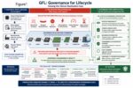
AI can compress the path to tape-out. The next challenge is compressing physical realization.
Something important is beginning to happen in semiconductor development: the design cycle itself is becoming compressible.
AI-assisted engineering can accelerate architecture exploration, RTL development, verification, physical… Read More
COMPANY EMAIL REQUIRED FOR REGISTRATION.
Studies show that nearly 20% of the verification cycle is spent on assertion generation, debugging, and methodology integration — work that remains largely manual today or is delegated to general-purpose LLMs that hallucinate more than 30% of the time and produce incorrect assertions.… Read More
Lance Hacking, Intel
Intel Core Series 3, code-named Wildcat Lake, is a mainstream client system-on-chip derived from the Panther Lake-based Core Ultra Series 3 architecture. Its design objective is not maximum feature density, but broad deployment of current-generation CPU, graphics, AI, memory, security, and connectivity… Read More
Join Us to Connect, Collaborate, and Shape the Future of AI
Get ready to immerse yourself in the future of semiconductor design at the 2026 TSMC Global Open Innovation Platform® (OIP) Ecosystem Forum! This isn’t just an event—it’s the ultimate collaborative hub where the world’s leading technology pioneers gather to discuss… Read More
The Silicon Gold Rushby Admin on 08-23-2026 at 11:59 pm
Are AI chips the new frontier of computing? What happens when the world’s biggest cloud companies stop buying chips and start designing their own?
In this program, we’ll unpack how companies once defined by software are… Read More
The semiconductor industry has achieved extraordinary mastery in silicon signoff. Modern EDA environments can now optimize timing closure, physical verification, IR/EM behavior, routing density, thermal interaction, and increasingly even design-space exploration through AI-assisted implementation flows. Crossing… Read More
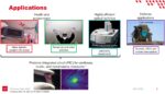
Mid-infrared (MIR) photonic integrated circuits are emerging as a key technology for applications ranging from environmental monitoring and medical diagnostics to defense and industrial process control. The MIR spectral region, often referred to as the molecular “fingerprint” region, exhibits strong absorption features… Read More