For years, advanced packaging has been described mostly in planar terms: chiplets placed side by side, connected through interposers, bridges, redistribution layers, substrates, and short-reach electrical links. This view remains important. It supports today’s GPU, HBM, chiplet, and 2.5D integration architectures.… Read More
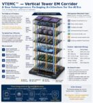
Tag: 2.5D integration
Intel: Pushing EMIB Forward: Design Methodology Insights with Synopsys Tools
As advanced packaging becomes a critical enabler for next-generation semiconductor products, Intel continues to drive innovation through its Embedded Multi-die Interconnect Bridge (EMIB) technology. EMIB has emerged as a foundational packaging solution for heterogeneous integration, allowing multiple chiplets and… Read More
Beyond Tool Interoperability: The Emerging Governed Convergence Problem in Semiconductor Design
The semiconductor industry has spent decades optimizing tools. Today, however, the central challenge is no longer whether individual tools are powerful enough. The real question is whether increasingly specialized tools, domains, models, and organizations can still converge coherently into a manufacturable, reliable,… Read More
