





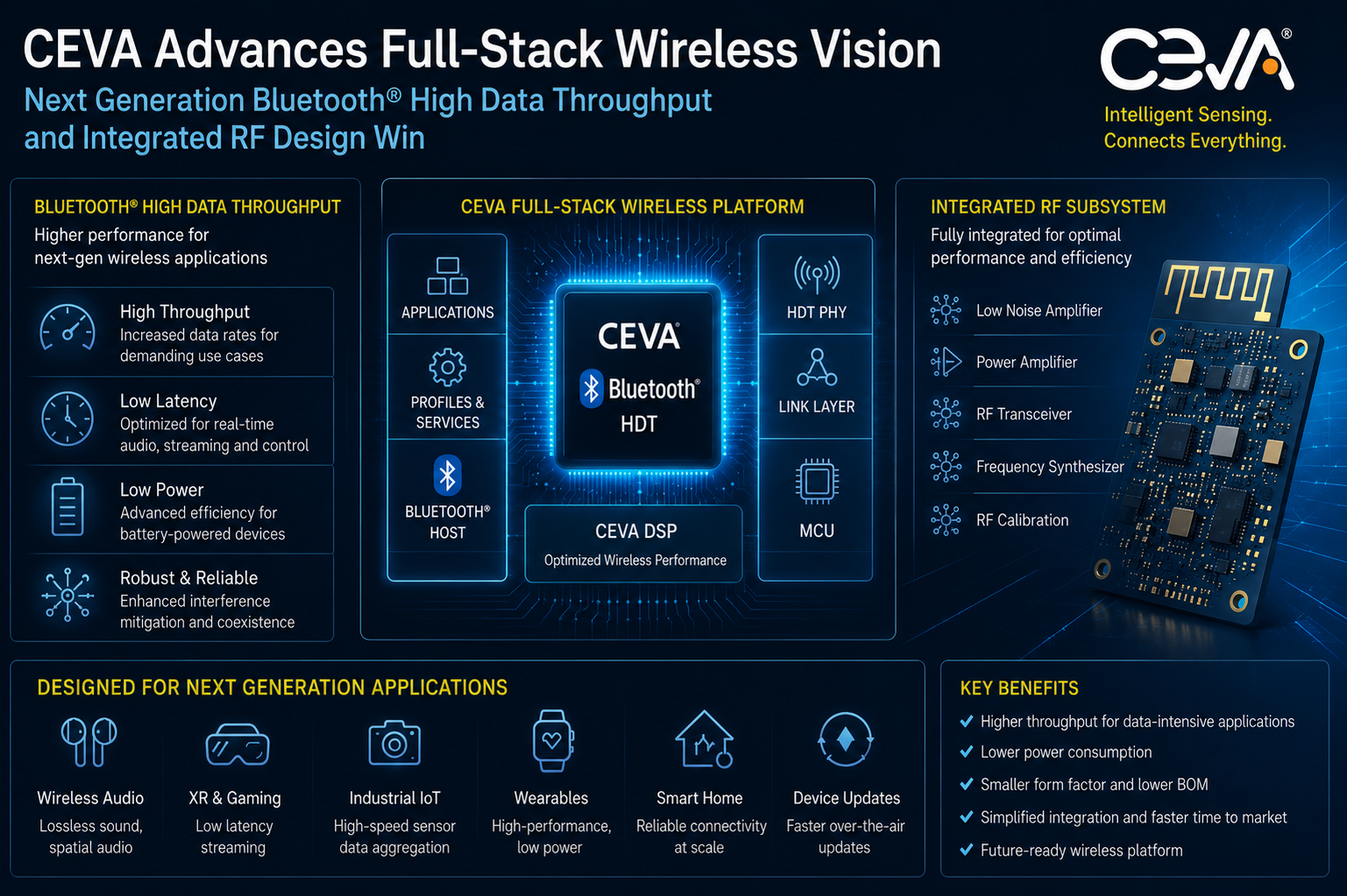
CEVA, the leading licensor of wireless connectivity and smart sensing technologies, is advancing its full-stack wireless strategy with the introduction of next-generation Bluetooth High Data Throughput (HDT) capabilities and a major integrated RF subsystem design win. The announcement underscores CEVA’s growing role in enabling highly integrated wireless SoCs for consumer, industrial, automotive, and IoT applications where performance, power efficiency, and silicon integration are becoming critical competitive differentiators.
Bluetooth technology is entering a new era as demand accelerates for higher bandwidth wireless audio, spatial computing, gaming peripherals, industrial edge devices, and AI-enabled wearables. While traditional Bluetooth Low Energy (BLE) has focused primarily on ultra-low-power communications, emerging applications increasingly require significantly higher throughput without sacrificing battery life. CEVA’s latest Bluetooth platform directly addresses this challenge through a scalable architecture that combines advanced baseband processing, optimized protocol stacks, and tightly integrated RF design.
At the center of CEVA’s strategy is support for Bluetooth High Data Throughput, an emerging capability designed to dramatically increase wireless data rates compared to conventional BLE implementations. HDT enables new classes of applications including lossless wireless audio, low-latency XR streaming, multi-stream sensor aggregation, and high-speed firmware updates. These use cases require not only enhanced PHY performance, but also intelligent coexistence management, adaptive scheduling, and advanced interference mitigation.
CEVA’s full-stack wireless approach integrates digital signal processing, modem IP, software protocol stacks, and RF subsystem technology into a unified platform. This architecture simplifies SoC development for semiconductor companies by reducing integration complexity and accelerating time-to-market. Rather than sourcing Bluetooth stack software, DSP cores, and RF IP from multiple vendors, customers can deploy a pre-validated CEVA platform optimized across all wireless layers.
A key aspect of the announcement is CEVA’s integrated RF design win, which validates the company’s strategy of moving beyond standalone IP licensing toward complete wireless subsystem solutions. Historically, many semiconductor companies have relied on discrete RF front-end development combined with externally sourced digital connectivity IP. However, advanced process nodes and increasingly compact device form factors are driving the need for deeper RF-digital co-optimization.
The integrated RF subsystem combines low-noise amplifiers, power amplifiers, frequency synthesizers, RF transceivers, and calibration technologies with CEVA’s Bluetooth baseband and software stack. This level of integration improves power efficiency, reduces board area, lowers BOM cost, and simplifies certification requirements. It also enables tighter control over RF performance metrics such as sensitivity, adjacent channel rejection, and coexistence with Wi-Fi and ultra-wideband radios.
The design win itself represents an important milestone because it demonstrates growing customer demand for turnkey connectivity platforms rather than isolated IP blocks. Semiconductor vendors targeting wearables, hearables, smart home devices, and industrial IoT products increasingly seek integrated wireless solutions that reduce engineering risk while enabling rapid product differentiation.
Bluetooth HDT is especially important for the wireless audio market, where higher-quality codecs and spatial audio experiences require more bandwidth than conventional Bluetooth architectures can efficiently deliver. CEVA’s platform supports advanced audio processing pipelines alongside optimized transport layers capable of sustaining higher throughput with deterministic latency. This is increasingly relevant as device makers compete to deliver premium audio experiences with lower power consumption.
Another important market driver is edge AI. Smart cameras, industrial sensors, and wearable health devices are generating significantly larger data streams that must be transmitted efficiently between devices and edge processors. Bluetooth HDT provides a compelling low-power alternative for short-range high-bandwidth communications, particularly in applications where Wi-Fi power consumption may be excessive.
From a technical perspective, CEVA’s expertise in DSP architectures gives the company a unique advantage in wireless connectivity. Signal integrity, channel equalization, interference suppression, and adaptive modulation all require substantial real-time processing capability. CEVA’s specialized DSP cores are optimized for these workloads while minimizing silicon area and energy consumption.
The company’s broader strategy aligns with an industry-wide shift toward platform-based semiconductor development. As wireless standards become more complex, OEMs and chipmakers increasingly prefer validated subsystem solutions that combine hardware, software, and RF technologies. This reduces integration cycles and allows engineering teams to focus on application-level innovation rather than low-level wireless implementation.
The integrated RF design win also highlights the importance of analog and mixed-signal expertise in next-generation wireless systems. While digital integration often receives the most attention, RF performance remains one of the most difficult challenges in advanced wireless SoCs. Variability across process nodes, antenna constraints, thermal considerations, and coexistence requirements all place pressure on RF subsystem design.
Bottom line: By combining Bluetooth HDT innovation with integrated RF technology, CEVA is positioning itself as a strategic enabler for the next generation of connected intelligent devices. As wireless applications continue evolving toward higher bandwidth, lower latency, and greater energy efficiency, semiconductor companies will increasingly require tightly integrated full-stack connectivity solutions. CEVA’s latest advancements demonstrate how the company is expanding beyond traditional IP licensing into comprehensive wireless platform enablement for the AI-driven edge computing era.
For more information, visit https://www.ceva-ip.com/
Also Read:
All in One Bluetooth Audio: A Complete Solution on a TSMC 12nm Single Die
From Satellites to 5G: Ceva’s PentaG-NTN™ Lowers Barriers for Terminal Innovators
Ceva IP: Powering the Era of Physical AI
Share this post via:



Comments
There are no comments yet.
You must register or log in to view/post comments.