




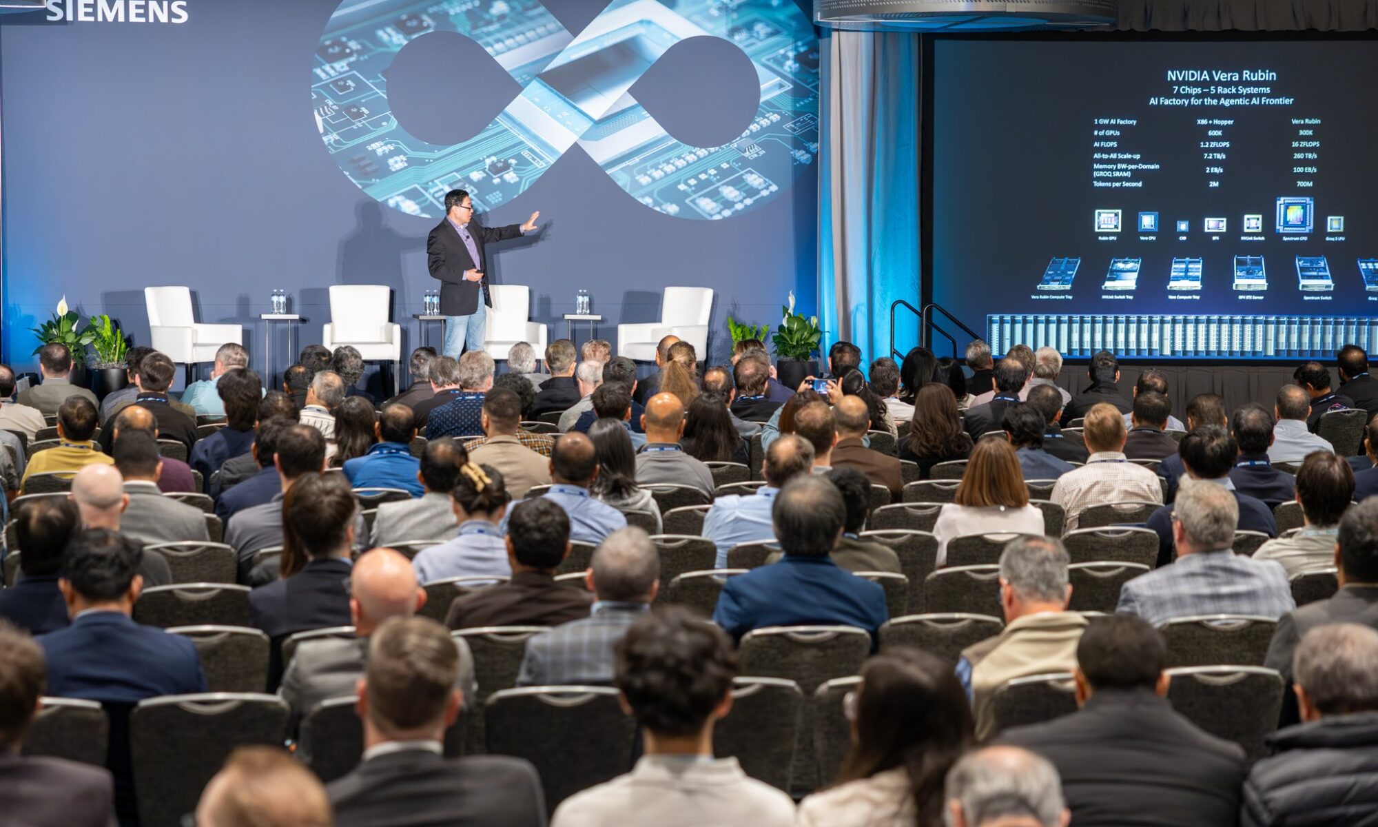

The semiconductor industry is entering a transformative new phase, driven by the convergence of artificial intelligence, cloud computing, and increasingly complex chip architectures. That message took center stage during the keynote talks at the Siemens EDA User2User 2026 North America conference. Executives from Siemens, NVIDIA, and Amazon Web Services described how engineering itself is being reshaped by AI-powered workflows and hyperscale infrastructure.
The conference highlighted a growing realization across the industry: semiconductor design is no longer just about building faster chips. It now requires engineers to think at the level of systems, software, physics, manufacturing, and even autonomous machines.
From Traditional EDA to System-Level Engineering
Opening the event, Jeff Applebaum reflected on how dramatically engineering has evolved over the past few decades. Early chip design relied heavily on manual processes and limited tooling. Today, engineers are working on designs that are exponentially more complex, while also facing pressure to deliver products faster than ever before.
That shift was expanded upon by Jean-Marie St. Paul, who emphasized that hardware innovation has once again become central to the technology industry. As AI workloads grow and advanced packaging technologies such as 3D ICs become mainstream, chip designers must now consider thermal behavior, mechanical stress, power delivery, and system-level integration alongside traditional logic and verification challenges.
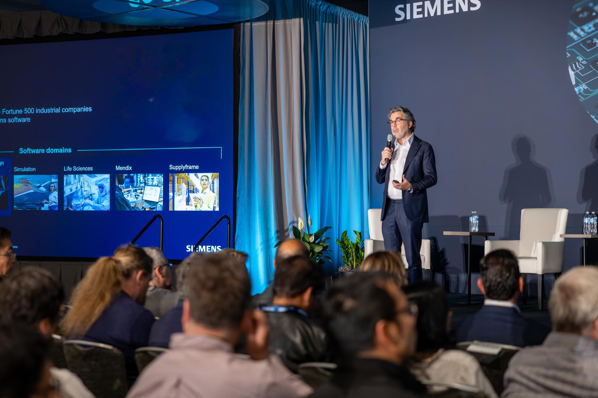
According to Siemens, this is fundamentally changing the role of EDA. The future of semiconductor development extends beyond schematic capture and simulation into areas such as digital twins, thermal modeling, industrial automation, and mechanical simulation. Semiconductor devices are increasingly being designed as part of larger intelligent systems rather than standalone components.
Siemens positioned itself as uniquely suited to support this transition because of its broader industrial portfolio, which spans software, automation, manufacturing infrastructure, and simulation technologies. The company’s long-term strategy is to connect the entire product lifecycle from chip design all the way to factory deployment through integrated digital workflows.
AI Becomes an Engineering Platform
Artificial intelligence was the dominant theme of the conference, particularly during the keynote by Da Yang of NVIDIA. He described AI not simply as a productivity tool, but as the foundational infrastructure for the next industrial revolution.
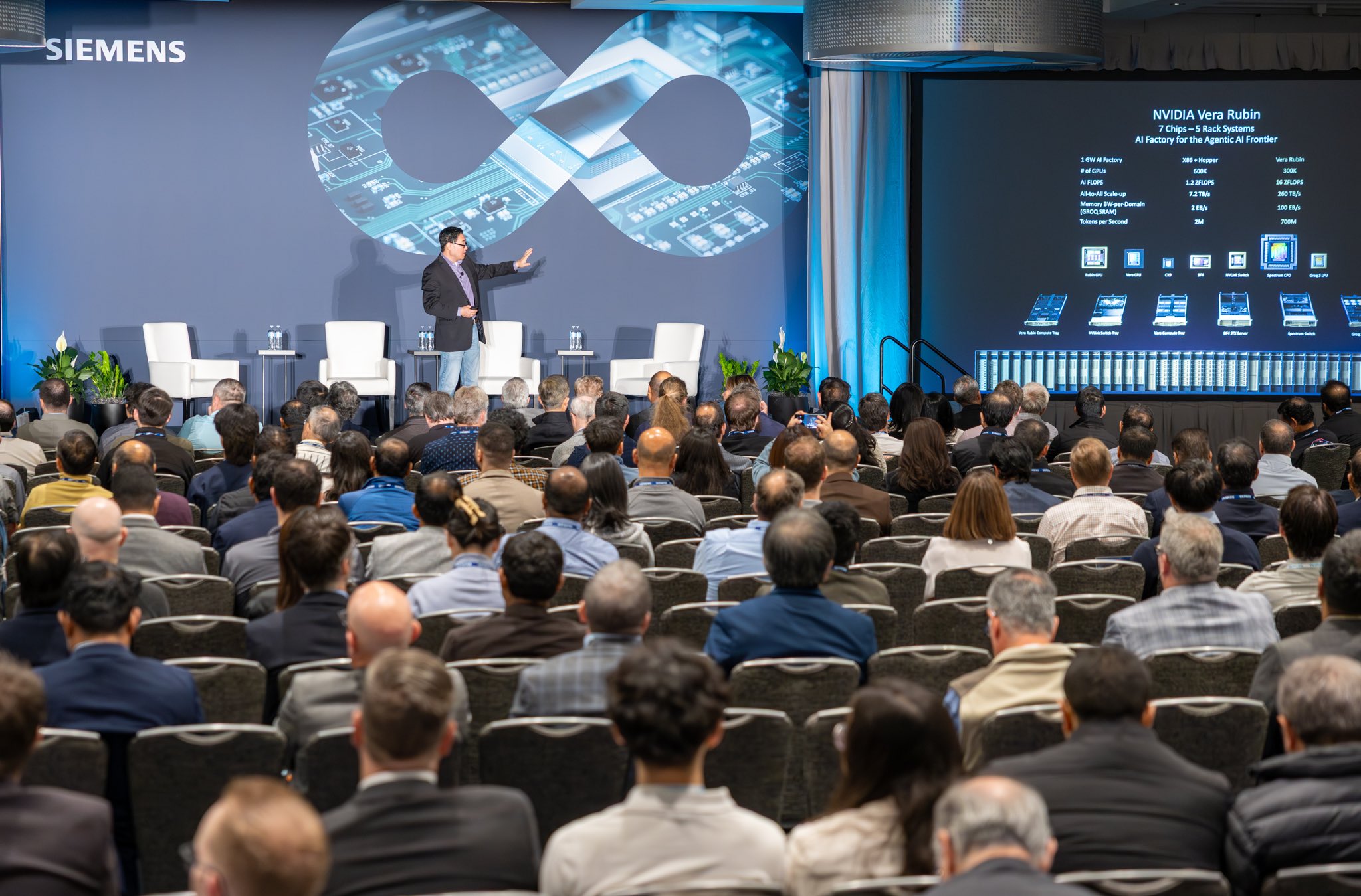
NVIDIA’s vision centers on a layered AI ecosystem built on accelerated computing. At the infrastructure level are massive GPU-powered supercomputers designed to train and run AI models at unprecedented scale. On top of that sits a growing stack of CUDA libraries, frameworks, and domain-specific AI applications tailored to industries such as semiconductor design and manufacturing.
These technologies are already producing significant gains in EDA workflows. NVIDIA highlighted major acceleration in tasks such as SPICE simulation, optical proximity correction, and parasitic extraction. Workloads that previously consumed hours or even days can now be completed dramatically faster through GPU acceleration and AI-assisted optimization.
But the larger shift lies in how AI interacts with engineers. The industry is moving beyond generative AI into what NVIDIA described as “agentic AI”. Such agentic systems are capable of reasoning, planning, and autonomously executing engineering tasks.
Instead of simply responding to prompts, these AI agents can coordinate workflows, analyze results, optimize designs, and interact with multiple engineering tools with minimal human intervention. The goal is not to replace engineers, but to augment their productivity and allow them to focus on higher-level problem solving.
This evolution is already beginning to reshape EDA workflows. AI copilots embedded into engineering tools can help automate repetitive tasks, accelerate debugging, and improve decision-making throughout the design process.
From Digital Intelligence to Physical AI
NVIDIA also introduced its broader vision for “physical AI,” which extends artificial intelligence into the real world through robotics, factory automation, and intelligent infrastructure.
The concept relies heavily on digital twins and simulation environments. Engineers can train AI systems in virtual environments that accurately replicate physical systems before deploying those models into factories, robots, or industrial equipment.
This approach has major implications for semiconductor manufacturing. AI-driven systems could optimize production lines, identify defects in real time, improve process control, and automate large portions of fab operations. NVIDIA described this as the beginning of a new industrial era in which AI moves beyond software applications and becomes embedded into physical operations.
The partnership between NVIDIA and Siemens is central to this vision. By integrating NVIDIA’s AI frameworks and Omniverse simulation technologies into Siemens’ industrial and EDA platforms, the companies aim to create end-to-end workflows that connect chip design, simulation, manufacturing, and deployment.
The Rising Cost of Delay
While NVIDIA focused on AI and intelligent systems, Nafea Bshara from AWS’s Annapurna Labs addressed another major industry challenge: time-to-market.
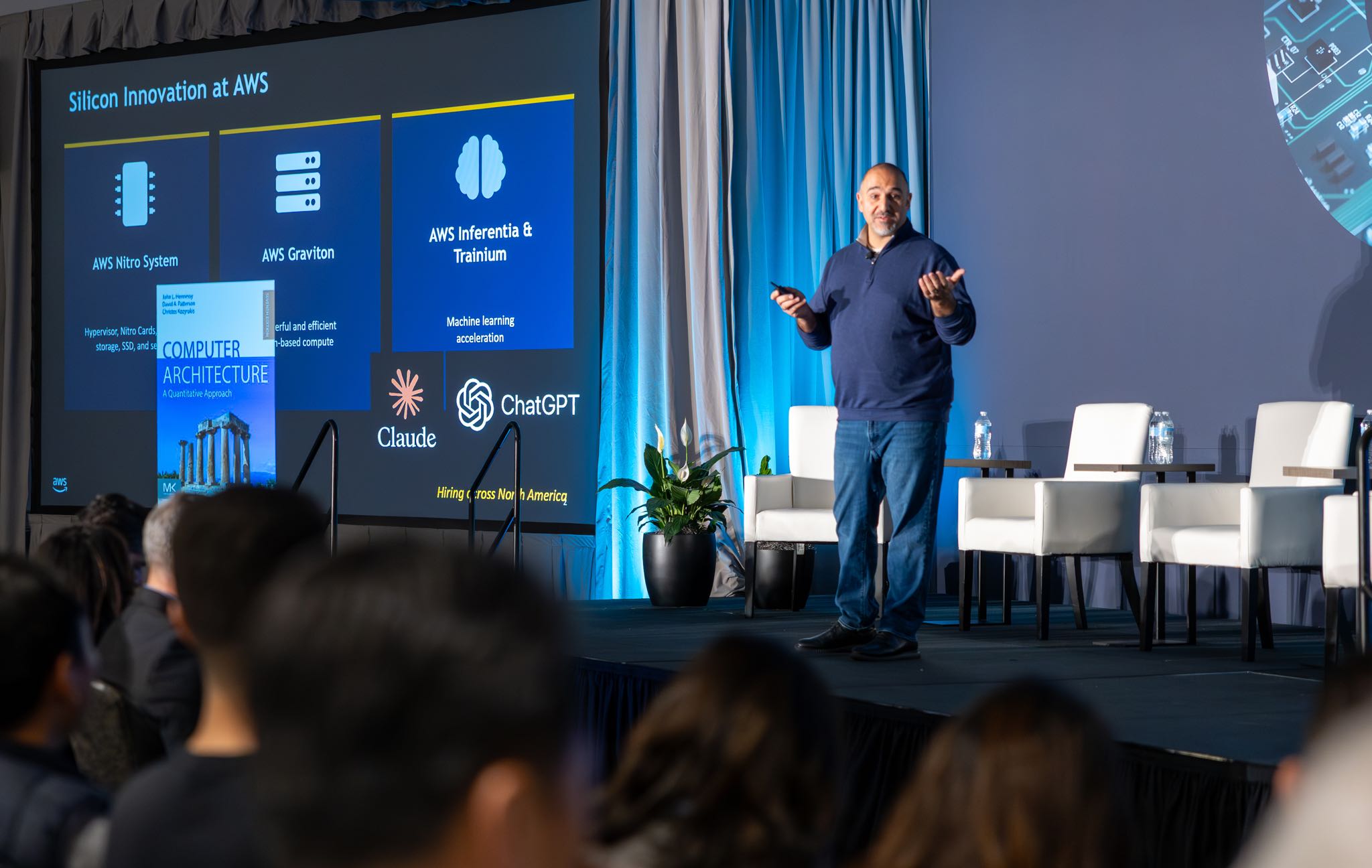
Bshara argued that in the AI era, even a small delay in delivering a new chip generation can create enormous financial consequences. As AI hardware generations increasingly deliver 2× or greater performance improvements, infrastructure operators cannot afford to remain on older platforms for extended periods.
A single-quarter delay, he explained, can translate into billions of dollars in wasted capital expenditures, increased energy consumption, and reduced efficiency at hyperscale data center operators.
This pressure is forcing semiconductor companies to rethink how they develop chips. Traditional on-premises compute infrastructure often cannot scale quickly enough to support modern design workloads, especially during peak verification and signoff periods.
Why the Cloud Matters for EDA
AWS presented cloud infrastructure as a solution to these bottlenecks. The company described what it calls “speed-of-light” chip development, where engineering teams can instantly scale compute resources based on workload demands.
Rather than waiting for limited on-premises servers, engineers can launch thousands of cloud instances in minutes, dramatically reducing queuing delays and improving iteration speed.
AWS also emphasized the importance of optimizing EDA tools for distributed and parallel execution. Working closely with Siemens EDA, AWS has helped accelerate key workloads such as design rule checking and simulation across large-scale cloud environments.
The result is faster turnaround times, more engineering iterations per day, and shorter overall development cycles. According to AWS, this flexibility is especially important as chip complexity continues to rise and AI workloads demand ever-larger verification runs.
Bshara also challenged the perception that cloud computing is prohibitively expensive for semiconductor development. In many cases, cloud infrastructure represents only a small percentage of total design costs while providing significant productivity gains and faster time-to-market.
Redefining the Engineer’s Role
Despite the emphasis on automation and AI, the conference repeatedly reinforced the importance of human engineers. AI systems may accelerate workflows and automate tasks, but engineers remain responsible for defining problems, validating outcomes, and making critical architectural decisions.
What is changing is the nature of engineering work itself. Engineers are increasingly becoming orchestrators of intelligent systems rather than operators of isolated tools. Success now requires expertise that spans hardware, software, AI, cloud infrastructure, and system-level design.
The industry is also becoming more collaborative. Semiconductor innovation increasingly depends on partnerships between EDA vendors, cloud providers, AI companies, foundries, and system integrators. The keynote presentations from Siemens, NVIDIA, and AWS collectively underscored how interconnected the ecosystem has become.
Summary
The Siemens EDA User2User conference offered a clear view of where the semiconductor industry is headed. AI is becoming deeply integrated into engineering workflows. Cloud infrastructure is removing traditional compute limitations. Digital twins and simulation environments are connecting virtual models with physical systems. And intelligent automation is beginning to transform manufacturing itself.
The result is a new model of engineering that is faster, more connected, and increasingly autonomous.
For semiconductor companies, the challenge is no longer simply building better chips. It is learning how to operate within a rapidly evolving ecosystem where AI, cloud computing, and physical infrastructure are converging into a single intelligent platform for innovation.
Also Read:
Library Characterization gets a Boost from AI
Europe is Getting Serious About ASIC Innovation
Siemens EDA Expands AI and Advanced Packaging Collaboration with TSMC
Share this post via:



Comments
There are no comments yet.
You must register or log in to view/post comments.