





With over a trillion chips manufactured every year and application requirements evolving faster than ever (across automotive, HPC, and AI), the pressure on SoC design teams has never been higher with design space keeps growing and schedules keep shrinking.
Indeed, for a complex SoC project, the number of possible configurations to evaluate can reach into the millions, with parameters that are deeply interdependent with objectives (power, performance, area, time-to-market) that are fundamentally in tension from one to another. Manual or semi manual design exploration, even when supported by experienced architects, remains highly complex.
Today we present the SoC PLANNER design solution which has reached the end of its R&D development stage after three years of collaborative work. SoC PLANNER addresses this gap. Funded by BPI France, SoC PLANNER provides a breakthrough design exploration solution which starts from the KPI and SoC design data to explore right to both RTL design implementation and design verification flows. These open new possibilities since it shortcuts many of the iterations between SoC design architects and both design implementation and design verification teams.
The SoC PLANNER R&D project brings together several technologies with complementary expertise from French research lab CEA, EDA software companies, Defacto Technologies and Innova Advanced Technologies. By integrating CEA’s A-DECA (Automated Design space Exploration for Computing Architectures), Defacto’s SoC Compiler, and Innova’s PDM (Project and Design Management) into a unified platform.
A-DECA allows automated exploration & optimization of computing architectures. SoC Compiler enables RTL generation and PDM, the management and planification of complex EDA flow. From automated design space exploration to the generation of the RTL ready for both logic synthesis and design verification, SoC PLANNER covers the full upstream pre-synthesis design chain, while uniquely considering an eco-design footprint score as part of the design exploration step. For large SoC design projects, the outcome is a measurable reduction in design cycles, resource consumption, and time to first silicon.
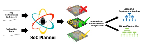
The SoC PLANNER design solution is made simple and intuitive. A user simply provides design parameters, including the ranges to explore and the targeted KPIs. Also, a user can set up the various metrics and whether the priority is low power, performance, area efficiency, or a balanced trade-off between them. From there, the design exploration engine takes over autonomously, estimating area, performance (bandwidth, latency, etc.) and power across the configuration space, it generates automatically filtered configurations along with their corresponding RTL code, bridging the gap in a single, seamless flow between architectural exploration and design implementation in the SoC PLANNER platform. As a notable addition into the SoC PLANNER-based flow, to each design configuration an eco-design footprint score is assigned. To our knowledge, this metric is unique in the chip design space and can be also considered into the exploration strategy.
A first version of the SoC PLANNER solution is ready for validation by early adopters offering to design teams beyond PPA exploration the immediate access to sustainability-aware design configurations. In the following sections, SoC PLANNER flow is illustrated through two use cases: a low power subsystem for a deep neural network, and an HPC (High Performance Computing) SoC subsystem.
SoC PLANNER-based Design Exploration: Low Power Use Case
This use case focuses on PNeuro, a programmable and energy-efficient architecture for deep neural network (DNN) inference acceleration in embedded edge AI systems. The platform combines a host processor, shared memory, and a scalable multi-cluster accelerator composed of configurable Neural Compute Blocks (NCBs), enabling exploration of performance, power, energy, and silicon area trade-offs.
The architecture exposes a large design space including cluster organization, memory hierarchy, clocking, bandwidth, and memory access characteristics. These parameters are evaluated against key industrial metrics such as inference latency, power consumption, energy efficiency, and implementation area.
SoC PLANNER starts with the fully autonomous exploration, running multi-objective analysis across the entire parameter space to identify the Pareto-optimal configurations. The results consistently show configurations that cut latency and energy in tandem, keeping both dynamic and static power in check. The top-ranked configurations were then then automatically translated into RTL, ready for synthesis and simulation.
The automated flow provided a 30–40% reduction in exploration time compared to manual evaluation, which represents a significant productivity gain. Beyond time savings, the Pareto analysis gives design teams a structured view of the trade-off landscape, enabling KPI-driven selection rather than an experience-based design process.
SoC PLANNER-based Design Exploration: HPC Use Case
As a second validation, an HPC SoC is considered. The architecture is built on the top of a scalable network-on-chip connecting a variable number of CPUs with multiple peripheral IPs, including memory controllers and I/O interfaces. The design space contains hundreds of possible configurations, including parameters such as the number of cores, cache sizes, and external memory and controller settings. The objective is to identify the best trade-off configurations across various KPIs including throughput, latency, and power.
After the exploration, the Pareto front identified configurations that optimally balance the target KPIs within the defined constraints, clearly separating optimal solutions from non-viable ones across the search space. The best RTL configurations are then automatically generated.
One of the key outcomes of this use case is the significant gain in exploration efficiency and engineering productivity. While exhaustive manual evaluation of hundreds of configurations would require around 150 hours, SoC PLANNER identifies optimal solutions in less than 2 hours, achieving a 75× speedup.
The generated results were validated against existing industrial design flows, demonstrating both the accuracy of the KPI estimations and the relevance of the selected configurations.
In summary, SoC PLANNER offers a concrete answer to one of the industry’s most pressing challenges. For both use cases, SoC PLANNER delivers what traditional methodologies could not deliver: the ability to explore vast design spaces in much shorter time, leads to optimal configurations across conflicting objectives, and automatically produce RTL-ready outputs; all within a single, integrated flow.
Conclusion
Chip complexity is growing faster than the tools and teams, design costs at advanced nodes are climbing fast, and the window between architectural decision and silicon availability keeps compressing. Facing these challenges, incremental improvements to existing workflows are no longer enough. SoC PLANNER solution offers a concrete, validated response to these pressures. By unifying into a single flow design exploration engine, pre-synthesis, RTL generation tool, and eco-design scoring, it addresses key design selection challenges. The two presented use cases confirm a much faster design exploration and a direct path from KPIs to synthesis-ready RTL configurations.
This project is funded by BPI France and is part of the France 2030 program.
Also Read:
WEBINAR: Defacto’s SoC Compiler AI: Democratizing SoC Design with Human Language
Defacto at the 2025 Design Automation Conference #62DAC
SoC Front-end Build and Assembly
Share this post via:



Comments
One Reply to “SoC PLANNER: A New Generation of SoC Design Exploration Solution Managing Cost-effectiveness and Sustainability”
You must register or log in to view/post comments.