

While the quantum world revolves around quantum computing, (QC) there are a couple of other quantum technologies of note. I covered one of these, quantum communication, in a recent blog. Here I’ll introduce the other, quantum sensing. The goal is to use the high sensitivity of an individual quantum state to external factors such as magnetic fields, able to sense very small variations outside the range of traditional sensors. There are indications that at least some of these applications may be much closer to production-ready than QC.
Origins
Deep research methods aren’t particularly helpful here. Instead, I’ll reference the first implementation example in Building Quantum Computers, based on Nuclear Magnetic Resonance. In or around 1997 attempts were made to build QC’s using NMR to monitor precession frequencies in molecules such as chloroform in liquid suspension. These methods provided proof of concept but were completely unscalable. Nevertheless, NMR and similar techniques such as electron spin resonance are now proving effective in quantum sensing, as illustrated in this paper and this paper.
I certainly can’t claim an exhaustive review of quantum sensing techniques, however examples I have found cluster around nitrogen vacancy centers in synthetic diamond. This name confused me at first. What it means is a nitrogen atom replacing a carbon atom in the diamond lattice plus a vacancy in the lattice adjacent to the nitrogen atom. Valence electrons for a negatively charged state of this structure form a spin-triplet state in both ground and excited primary states (sorry, bit of physics) with 3 possible magnetic quantum states: 0 and ±1. The 0 state is (energetically) lower than the ±1 states and the ±1 states split further under influence of a magnetic field, the difference being proportional to the field strength.
Detecting spin states is accomplished through fluorescence from excited states. The 0 state on relaxing back to the ground state fluoresces brightly, the ±1 states fluoresce less brightly since they often relax through an intermediate state. Frequency sweeping microwave radiation pulses across the diamond changes populations between 0 and ±1, detectable as a dip in fluorescence at a frequency related to the magnetic field strength. Which proves very useful in semiconductor defect detection.
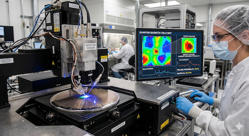
An application for failure analysis
Quantum Diamonds has just installed a production system at Eurofins EAG Labs in Sunnyvale, aimed to support failure analysis for <5nm tech and 3D packaging. This system was first unveiled at Semicon Taiwan in 2025 and is especially valuable for non-destructively testing for semiconductor shorts, leakage and opens in die and in 3DIC. The Quantum Diamonds Microscopy platform images magnetic fields generated by current flow in a chip and can achieve remarkable localization resolution: <1μm in xy and down to 1 μm in depth, with a 3mm x 3mm field of view (which can be stitched to larger areas).
There are several interesting aspects to this technology. The usual constraints on QC don’t apply here. While additional defect centers may be used to amplify light signal, there is no need for superposition or entanglement. This is a simple atomic physics application: pump electrons up to an excited state, observe fluorescence when they relax back to the ground state. Also the technology works at room temperature, no need for special cooling. Diamond is especially stiff, minimizing impact of heat noise, it has a wide bandgap minimizing electrical noise, and if diamonds are grown using isotopically pure C12, there is no nuclear “noise” from C13. This room-temperature capability makes quantum sensing interesting in other areas, such as a hack-proof alternative to GPS, based on detecting variations in the earth’s magnetic field.
You can read the Quantum Diamonds press release HERE and a more detailed paper for a different application HERE.
Also Read:
Panel Discission: Beyond Moore’s Law and the Future of Semiconductor Manufacturing
RISC-V: From Niche Architecture to Strategic Foundation
Bringing mathematical rigour in the world of hardware – a journey into Formal Verification
Share this post via:


Consolidation and Competition: Who is Winning the $4.5 Billion Interface IP Race?