 The Internet of Things (IoT) is creating urgent demand for a new generation of analog/mixed-signal (AMS) designs, some of which also contain MEMs. To efficiently create the myriad of AMS devices at the edge of the IoT requires a design environment that is affordable and easy to use, but powerful enough to create the widely diverse range of products needed for deployment in the IoT.
Though most of these devices will be inexpensive, there will lots of them – millions and soon billions of form-factors of every description, all created and deployed to gather analog information in the physical world. Wearables may be the media darlings at the moment but in fact examples range from traffic monitoring, smart meters and video surveillance for smart cities, to medical devices that monitor glucose levels, heart rates and mobility and everything in between. And don’t worry, chip designers. These devices will generate a tsunami of analog data that must be digitized and transmitted either to the desktop or to data centers for analysis on phablets, laptops, PCs and servers and systems – all of which contain the more expensive, higher-margin silicon that remains the bread and butter for our industry.
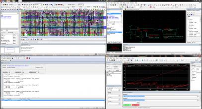
If you’re an AMS designer, you know all about the challenge that comes with creating mostly analog circuitry along with some digital—the so-called ‘Big A/little D’ designs that also can include MEMs functionality. A new generation of affordable, easy-to-use AMS design tools from Mentor Graphics called Tanner AMS IC Design flow is emerging that directly address these challenges, providing a complete flow tailored for the big-A/little-D AMS market for every stage of the design process as well as MEMs. These tools deliver myriad benefits, including increased automation, improved accuracy, lower NRE costs and reduced time to market.

It’s always a tough decision, however, when evaluating and adopting a new set of design tools and capabilities, especially for AMS design. That is why Mentor Graphics has created the Tanner AMS Virtual Lab. Now you can test drive Tanner tools online and experience firsthand how intuitively easy it is to use this powerful, fully integrated and cost-effective AMS design flow. The Virtual Lab covers all aspects of AMS design: schematic capture; mixed-signal simulation or co-simulation; digital synthesis with DFT support; analog place and route; and high-speed, “sign-off ready” timing analysis for tape-out along with MEMs design and layout.
All it takes to access the virtual lab environment is an updated Web browser. There’s no downloading, so no IT department approval is required. Sign up and access to the lab is available for 30 days.


Comments
0 Replies to “Test Driving Analog/Mixed Signal Design for the Internet of Things”
You must register or log in to view/post comments.